5. Adding fiber couplers: the final working circuit
In the previous sections, we have learned how to optimize a waveguide Bragg grating (WBG) to achieve maximal temperature sensitivity. Of course, the WBG cannot function on its own; it needs to communicate with an off-chip laser and detector. For this reason, we still need to connect input and output fiber grating couplers to the WBG. Secondly, we are interested in measuring the reflected signal from the WBG. Since this reflected signal will end up at the input grating coupler, we will need to use an external optical circulator in order to separate the forward propagating signal (the input light) from the reflected signal. Alternatively, we can also route part of the reflected signal on chip to another fiber grating coupler, thus obviating the need for an optical circulator to capture this signal. This is the strategy we decide to follow. Finally, since the input and output fiber grating couplers introduce a certain insertion loss and bandwidth limitation, we need to find a way to normalize the measured WBG spectra with the characteristic of these I/O ports.
Creating a functional circuit is thus the focus of this section, and we will dive into three topics:
Creating the circuit layout
Simulating the full circuit
Export the circuit to a gds file
5.1. Creating the circuit layout
As explained in the introduction, laser light or another light source is required to characterize the WBG. To couple this light into the WBG, we need to use fiber grating couplers as I/O ports. The SiEPIC PDK provides a pre-designed and tested fiber grating coupler that we can use for this purpose. This building block consists of a specially designed grating that efficiently converts incident light from a fiber into a waveguide mode in a certain wavelength range. Since the fiber is large (diameter of \(125\,\mathrm{\mu m}\)) compared to the grating coupler (ca. \(10-20\,\mathrm{\mu m}\) in diameter) and to comply with any packaging requirements (if necessary), we will place the grating couplers sufficiently far from each other. The minimum distance that the SiEPIC foundry requires is \(127\,\mathrm{\mu m}\). Sticking to this distance will also enable the use of fiber arrays, thus greatly simplifying the packaging and experimental characterisation.
The other requirements we mentioned were:
the need to normalise the measured spectra from the WBG due to the limited bandwidth of the I/O grating couplers and
the need to reroute part of the reflected optical signal to an I/O grating coupler other than the input port.
These two requirements can be met when employing a 2x2-splitter and the functionality is illustrated in Temperature sensor circuit.
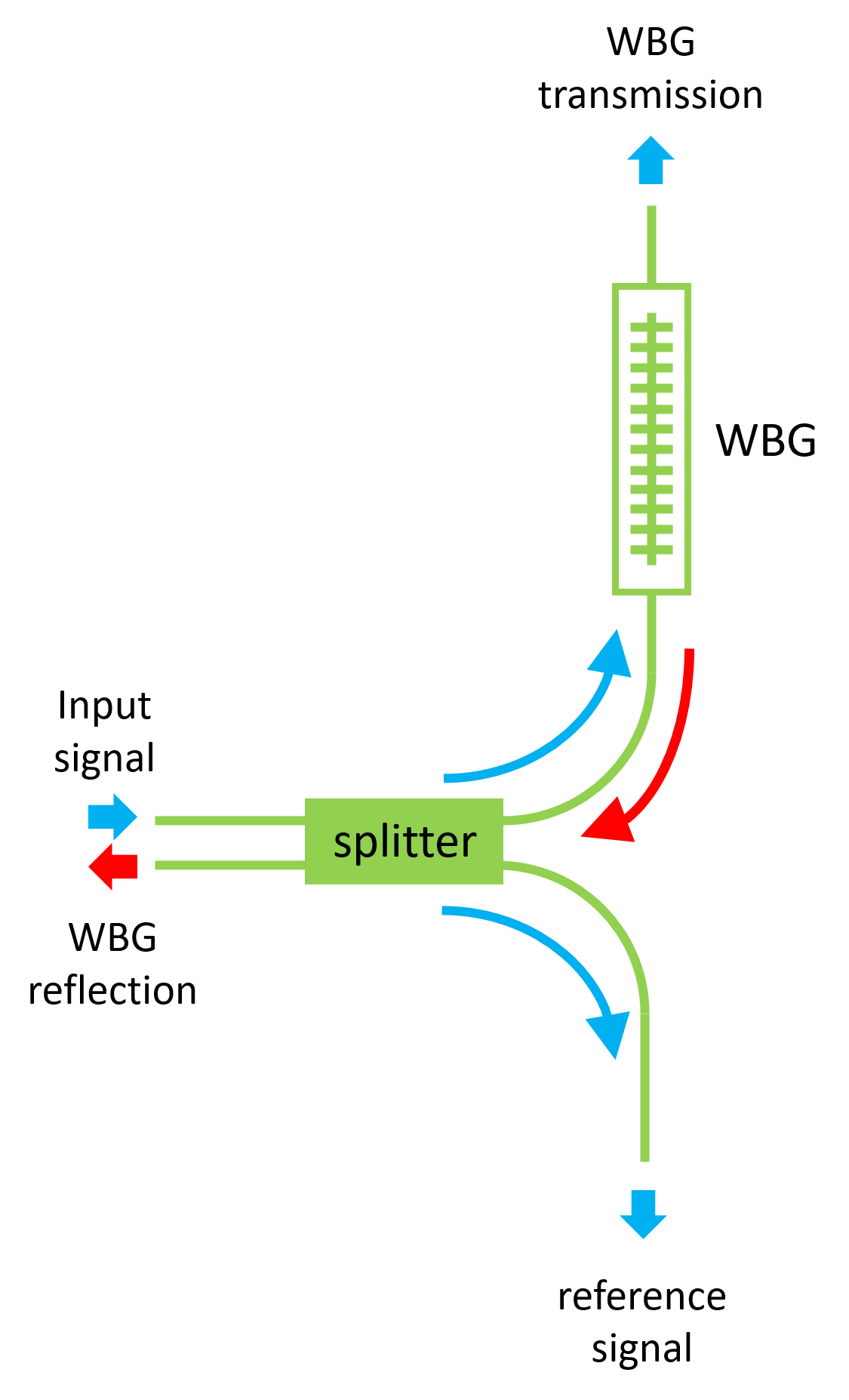
Functionality of the temperature sensor circuit.
Light from the input grating coupler will enter one of the input ports of the 2x2 splitter and split in two arms: an arm with the WBG and a reference arm without a WBG. The reflected signal arriving at the output ports of the 2x2 splitter will then be split over the splitter’s input ports. One of the input ports is already connected to the input grating coupler, but the other can be used to reroute part of the reflected signal to another grating coupler. As a result, we have four ports:
The input port to couple the light in
The output port to measure the transmission spectra of the WBG
The reference arm that measures the transmission spectra of two cascaded grating couplers
The output port to capture the reflection of the WBG
The reflection spectra from the WBG can thus be normalized to the transmission spectra from the reference arm. The SiEPIC PDK contains several 2x2-splitters. Among those, we choose to use the “adiabatic coupler” 2x2-splitter as it yields a relatively broadband response and has negligible reflections.
We now create a Python file (full_circuit_cells.py) that contains the class FullCircuit in which we will initiate all the required building blocks.
The code is given below:
class FullCircuit(i3.Circuit):
    wbg = i3.PCellProperty(doc="Unit cell of the WBG")
    fiber_coupler_pitch = i3.PositiveNumberProperty(doc="Distance between fiber grating couplers", default=127.0)
    bend_radius = i3.PositiveNumberProperty(doc="Bend radius of the connecting waveguides", default=10.0)

    def _default_specs(self):
        fc = pdk.EbeamGCTE1550()
        br = self.bend_radius
        fcp = self.fiber_coupler_pitch
        wbg_cell = self.wbg
        wbg_length = wbg_cell.get_default_view(i3.LayoutView).size_info().get_width()
        wbg_y_offset = (1.5 * fcp - wbg_length) / 2.0
        fc_names = ["fib_out_ref", "fib_out_wbg_r", "fib_in", "fib_out_wbg_t"]
        specs = [
            i3.Inst("wbg", self.wbg),
            i3.Inst(["fib_in", "fib_out_wbg_t", "fib_out_ref", "fib_out_wbg_r"], fc),
            i3.Inst("splitter", pdk.EbeamAdiabaticTE1550()),
            i3.Inst("floorplan", pdk.FloorPlan(size=(300.0, 3 * self.fiber_coupler_pitch + 29.0))),
        ]
        specs += [i3.Place(f"{fc}:opt1", (0, cnt * fcp)) for cnt, fc in enumerate(fc_names)]
        specs.append(i3.Place("splitter", (2 * br, -fcp / 2.0), relative_to="fib_in:opt1"))
        specs.append(i3.Place("wbg:in", (br, wbg_y_offset), angle=-90, relative_to="splitter:opt3"))
        specs.append(i3.Place("floorplan", (-50, -15), relative_to="fib_out_ref:opt1"))

        specs.append(
            i3.ConnectManhattan(
                [
                    ("fib_in:opt1", "splitter:opt1"),
                    ("splitter:opt3", "wbg:in"),
                    ("wbg:out", "fib_out_wbg_t:opt1"),
                    ("splitter:opt4", "fib_out_ref:opt1"),
                    ("splitter:opt2", "fib_out_wbg_r:opt1"),
                ],
                bend_radius=self.bend_radius,
                min_straight=0,
            )
        )

        return specs

    def _default_exposed_ports(self):
        return {
            "fib_in:fib1": "in",
            "fib_out_wbg_t:fib1": "wbg_t",
            "fib_out_wbg_r:fib1": "wbg_r",
            "fib_out_ref:fib1": "ref",
        }
Just as we did with the unit cells in the WBG, we create the instances containing all the necessary building blocks which for our circuit are:
Four I/O grating couplers
One splitter
One WBG
Connecting waveguides
Chip floorplan
This circuit is generated through i3.Circuit similarly to the splitter tree in Designing a splitter tree.
The difference is that, here, we use Manhattan bends for the connecting waveguides.
We also add the chip floorplan to the circuit, which determines the chip boundaries.
Although it is not connected to any functional circuitry (and so will give a warning when running example_full_circuit.py which can be ignored), it is necessary for the foundry to know where to dice the chip.
The input and output ports of the circuit are simply the vertical ports of the I/O grating couplers (fib1), but we rename them accordingly to their function: in, wbg_t, wbg_r and ref.
Now, we can simply instantiate and draw the full circuit with the following code in example_full_circuit.py:
width = 0.5
deltawidth = 0.088
dc = 0.2
lambdab = 0.325

uc = UnitCellRectangular(
    width=width,
    deltawidth=deltawidth,
    length1=(1 - dc) * lambdab,
    length2=dc * lambdab,
)

wbg = UniformWBG(uc=uc, n_uc=300)

full_circuit = FullCircuit(wbg=wbg)
full_circuit_lo = full_circuit.Layout()
full_circuit_lo.visualize(annotate=True)
In this piece of code, we first define the optimized unit cell and use it to instantiate the WBG PCell.
Finally, we pass on this WBG PCell to instantiate the FullCircuit class.
The layout is shown here in Full circuit layout:
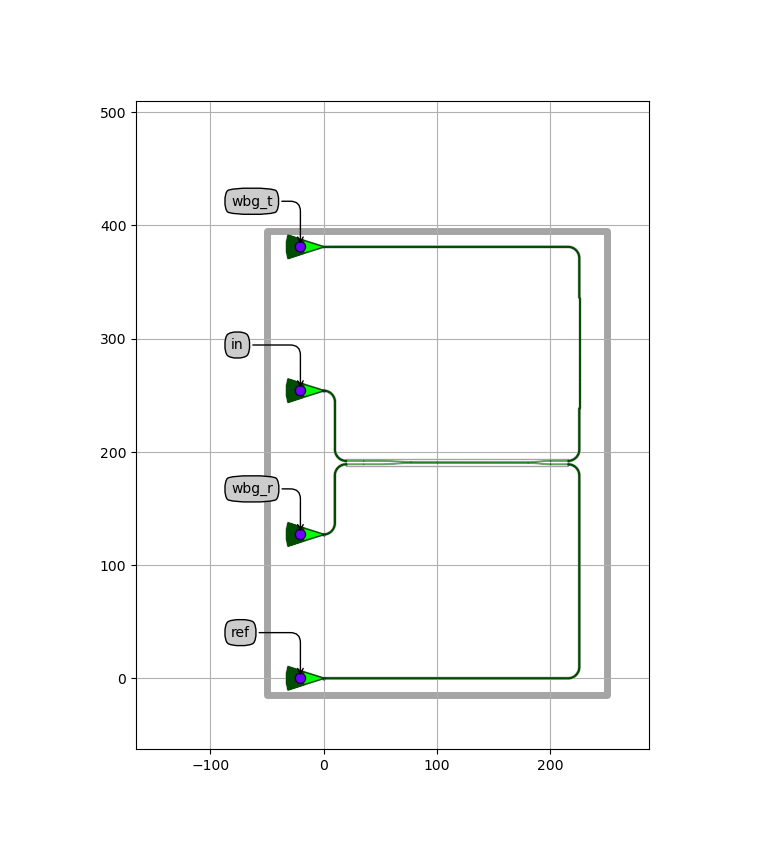
Full circuit, showing the grating couplers, splitter, WBG arm, reference arm and chip floorplan.
5.2. Simulating the final circuit
The circuit model of our temperature sensor is automatically generated from the layout through i3.Circuit.
In order to simulate the circuit at various temperatures, we need to explicitly pass on these temperatures to the get_smatrix method.
An example is given at the end of example_full_circuit.py:
temperatures = np.linspace(273, 373, 3)
wavelengths = np.arange(1.52, 1.58, 0.0001)

fig = plt.figure(constrained_layout=True)
gs = gridspec.GridSpec(1, 2, figure=fig)
axes_sparam = [fig.add_subplot(gs[0, 0]), fig.add_subplot(gs[0, 1])]

axes_sparam[0].set_xlabel(r"Wavelength (nm)", fontsize=16)
axes_sparam[0].set_ylabel("WBG Reflection (a.u.)", fontsize=16)
axes_sparam[0].set_title("Raw data", fontsize=20)

axes_sparam[1].set_xlabel(r"Wavelength (nm)", fontsize=16)
axes_sparam[1].set_ylabel("WBG Reflection (a.u.)", fontsize=16)
axes_sparam[1].set_title("Normalised data", fontsize=20)

full_circuit = FullCircuit(wbg=wbg)
full_circuit_cm = full_circuit.CircuitModel()

for temperature in temperatures:
    full_circuit_Smatrix = full_circuit_cm.get_smatrix(wavelengths=wavelengths, temperature=temperature)
    reflection = i3.signal_power(full_circuit_Smatrix["in:0", "wbg_r:0"])
    transmission_ref = i3.signal_power(full_circuit_Smatrix["in:0", "ref:0"])

    axes_sparam[0].plot(
        wavelengths * 1000,
        reflection,
        "o-",
        linewidth=2.2,
        label=r"Reflection at " + str(int(temperature - 273)) + r" $^{\circ}$C",
    )
    axes_sparam[1].plot(
        wavelengths * 1000,
        reflection / transmission_ref,
        "o-",
        linewidth=2.2,
        label=r"Reflection at " + str(int(temperature - 273)) + r" $^{\circ}$C",
    )

axes_sparam[0].legend(fontsize=14, loc=6)
axes_sparam[1].legend(fontsize=14, loc=6)
axes_sparam[0].tick_params(which="both", labelsize=14)
axes_sparam[1].tick_params(which="both", labelsize=14)
plt.show()
This script will calculate and plot the reflection spectra, both the raw data from the wbg_r port and the data normalized to the transmission of the reference arm, measured at the ref port.
This is done at three different temperatures (\(0^\circ \mathrm C\), \(50^\circ \mathrm C\) and \(100^\circ \mathrm C\)).
The results are depicted in WBG reflection spectra.
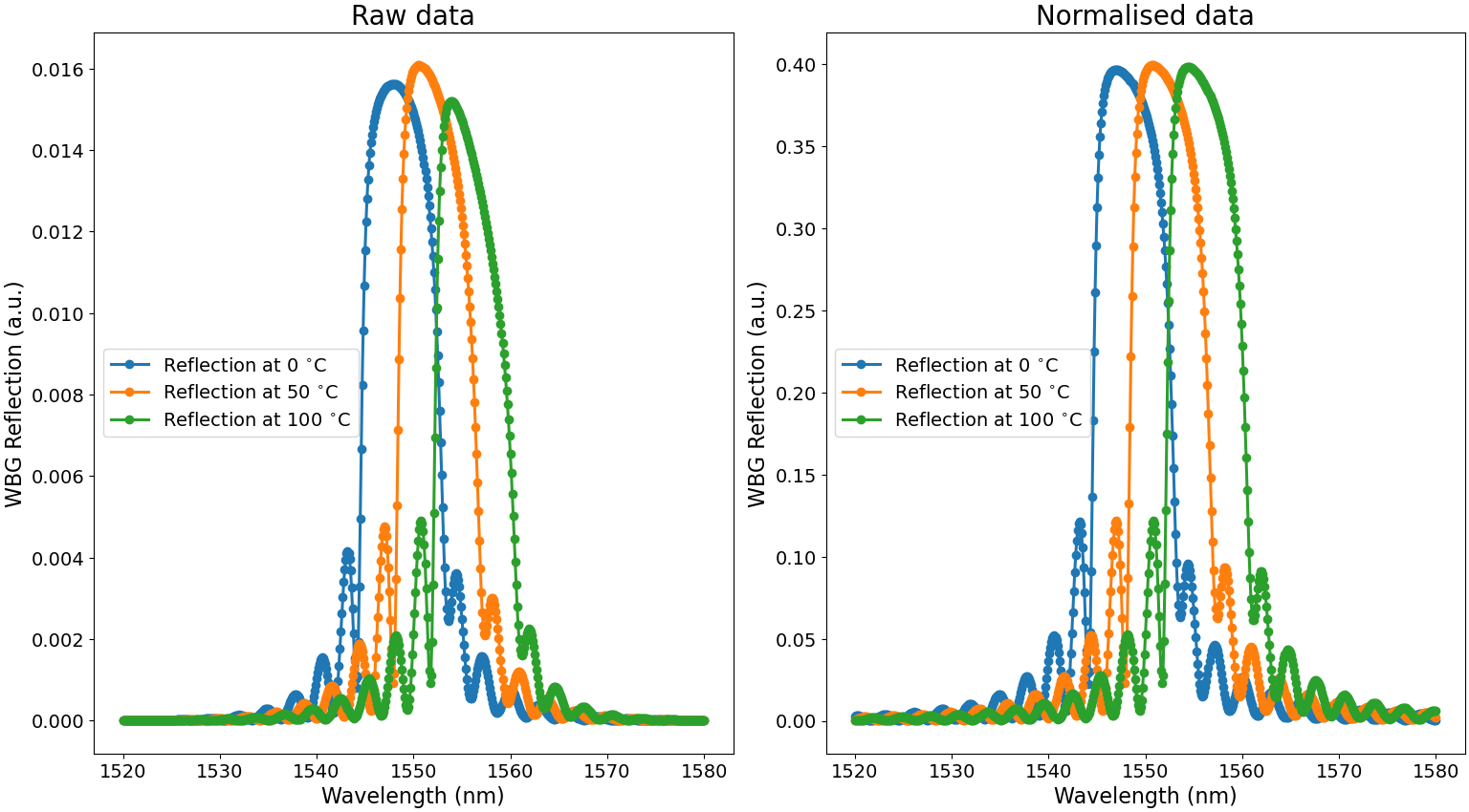
Reflection spectra from the WBG.
Left: raw transmission data from the wbg_r port.
Right: data from the wbg_r port normalised with the transmission measured from the reference arm at the ref port.
WBG reflection spectra illustrates the importance of adding the reference arm. As can be seen, due to the limited bandwidth of the grating couplers, the reflection spectra will get distorted for large temperature changes. This effect can be compensated by normalising the reflection spectra with the measurements from the reference arm as seen in the figure on the right.
It should be noted that, although in reality the behavior of the I/O ports will also change with temperature, this is not taken into account in the grating coupler model as the data was not available at the time of publishing this tutorial. Nevertheless, because we use normalized reflection spectra, the influence of temperature effects in the grating couplers is minimized. This once more illustrates the importance of using normalized data in order to obtain reliable measurements.
5.3. Exporting the final layout to a gds file
Now that the full circuit has been designed and numerically characterised, it is finally time to generate the gds file to be sent to the foundry for fabrication. This is very easy to do; simply write
full_circuit_lo.write_gdsii('full_circuit.gds')
at the end of example_full_circuit.py, and the gds-file of the circuit is generated in the directory where example_full_circuit.py is located.
You can always check this gds-file in KLayout as depicted in Circuit GDS.
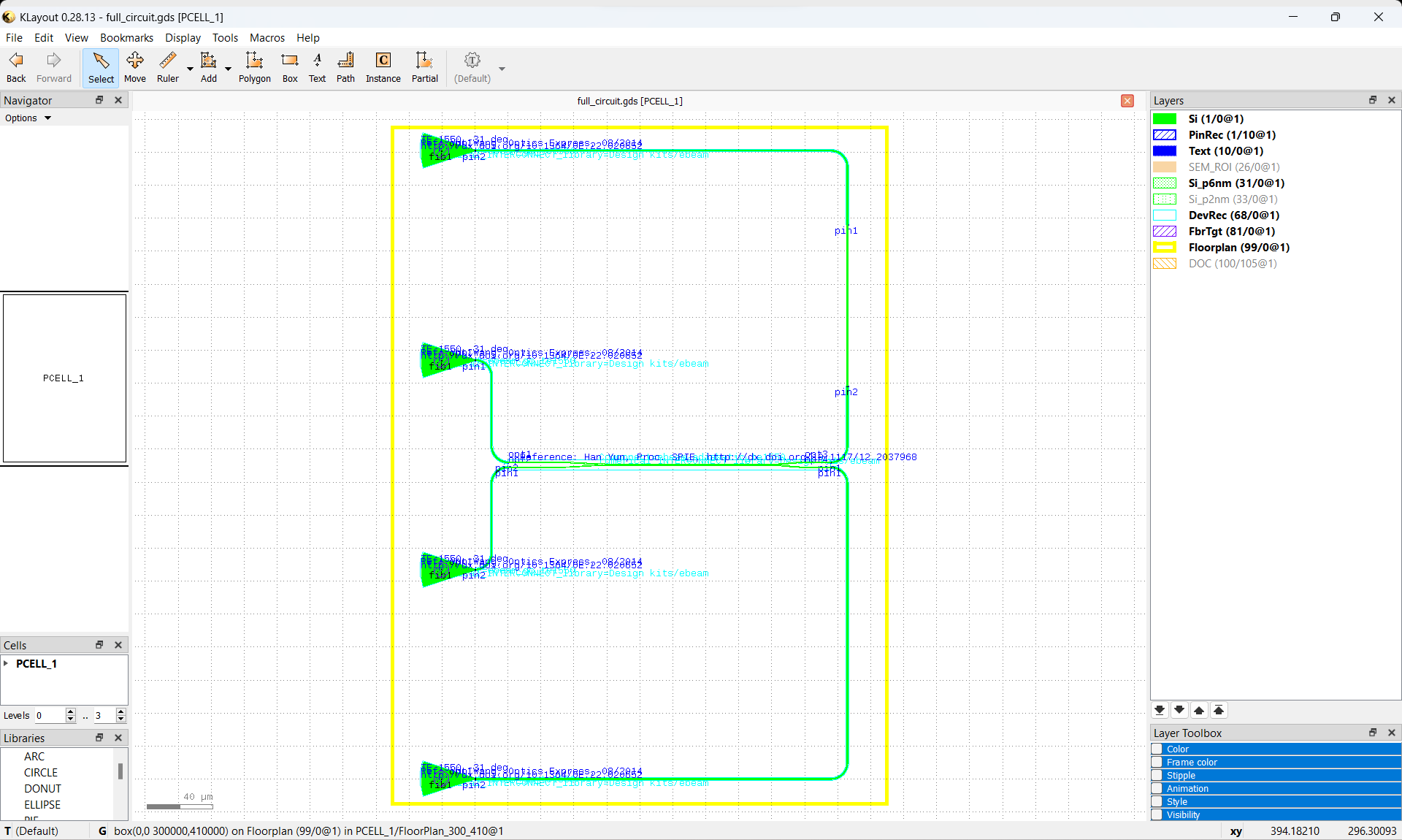
GDS of the full circuit in KLayout.
Now, you finally have the layout of a working temperature sensor, ready to be fabricated and packaged by the foundry!