Ligentec: Arrayed waveguide grating (AWG) for integrated optical coherence tomography
Note
This application example requires the Luceda PDK for Ligentec’s AN150 platform. Please contact Ligentec to obtain access to this PDK.
Introduction
Arrayed waveguide gratings (AWGs) are (de)multiplexing devices with a wide array of applications. One such application is optical coherence tomography (OCT) which is used in medical applications such as retinal imaging [1]. OCT can be described as an optical version of ultrasound imaging. In OCT, a broadband light beam is split into two beams. One of these beams penetrates into the object (such as a human retina) to be imaged and is reflected from it at a range of different depths [2]. The other beam is reflected from a reference mirror and follows a known path. The two reflected beams are then recombined, causing interference between them [2]. The frequencies of the recombined beam are then separated by a spectrometer, conventionally a diffraction grating [3]. Using the output of the spectrometer, one can then reconstruct the structure of the object at the range of depths in which it is imaged. By scanning the OCT system over the two transverse directions, a 3D image of the object can then be reconstructed.
![Set-up for OCT. Image from [4]_.](../../../_images/optical_coherence_tomography.png)
However, OTC is typically implemented using bulk optical components that are expensive and take a lot of space [1]. The solution is therefore to integrate the spectrometer component in an integrated circuit [1]. This is achieved by implementing that component with an AWG.
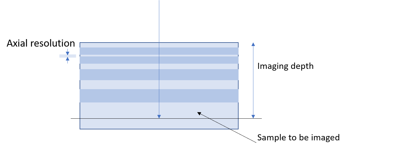
The performance of an OCT system is determined by several different metrics. Two of these metrics are the axial resolution and its imaging depth. The former describes how close together along the axial direction (i.e. along the depth) different parts of the object’s structure can be resolved. The latter describes how deeply an object can be imaged.
These metrics are both related to the specifications of the spectrometer, in this case the AWG, and of the light source. In particular, the axial resolution is inversely proportional to the effective bandwidth of the detected light. This depends on both the bandwidth of the light source and that of the AWG. This means that, provided that it remains smaller than the bandwidth of the light source, the greater the bandwidth of AWG, the finer the axial resolution [5] [6]. The maximum imaging depth, on the other hand, is directly proportional to the spectral sampling interval and thus the channel spacing [5] [6]. The practical imaging depth is, however, of also limited by the material properties (scattering and absorption) and the crosstalk, which we will explain later. This means that there is trade-off: if you reduce the channel spacing of the AWG, you will increase the imaging depth of the OCT system but you will reduce its axial resolution for the same number of output channels. To have high resolution and imaging depth, an AWG with a large number of output channels is needed. Fortunately, the Luceda AWG Designer is capable of helping you design and simulate such a large AWG.
In this application example, our goal is to implement such an AWG for OCT applications, using this paper [1] published by the Nature group as a reference. The AWG they have fabricated and characterized in that paper is already able to perform well enough for commercial applications. With the help of this tutorial, you will be able to fabricate such an AWG too. This AWG operates in the very near infrared region and so is fabricated in silicon nitride which is transparent in this region. It has 256 output channels around a central wavelength of 794 nm and a channel spacing of 0.09 nm.
As it takes time to implement and simulate such a large AWG, in this application example, we will begin by implementing an AWG with 64 output channels spaced 0.2 nm apart. You will be invited to change some parameters so as to see how the layout and light output of the AWG changes. In your own time, you may then decide to build the large AWG we show above.
Similarly to the Getting Started with Luceda AWG Designer and Organizing your AWG design project tutorials, in this application example we will go through the following steps:
- AWG generation
We will start by instantiating the subcomponents from the Ligentec PDK.
Then, we will synthesize the AWG, i.e. derive its implementation parameters.
Finally, we will assemble the AWG based on a U-shaped rectangular waveguide array.
- AWG simulation and analysis
In this step, we simulate the AWG we just assembled and then analyze its results to see how well it performs.
- AWG finalization
In the last step, we finalize the AWG design and route it to the edge couplers, so that it is ready for use.
These steps are all implemented in a number of custom functions: generate_awg, simulate_awg, analyse_awg and finalise_awg.
These functions are very similar to the functions of the same name in the Organizing your AWG design project tutorial and serve the same purpose.
A more detailed look on these functions can be seen in that tutorial.
As in the Organizing your AWG design project tutorial, we also have a script that we call example_generate_awg.py that calls these functions and goes through all these steps.
The script can be customized to skip certain steps, depending on the goal.
The full script can be found below.
import ligentec_an150.all as pdk  # noqa: F401
import ipkiss3.all as i3
import numpy as np
import os
from rect_awg.generate import generate_awg
from rect_awg.simulate import simulate_awg
from rect_awg.analyze import analyze_awg
from rect_awg.finalize import finalize_awg

# Actions
generate = True
simulate = True and generate
analyze = True
finalize = True and generate
plot_layout = False and generate
plot_sim_results = True
write_gds = True

# Specifications
center_wavelength = 0.800
channel_spacing = 0.2 * 1e-3
n_channels = 64
fsr_wavelength = (n_channels + 1) * channel_spacing

n_arms = None
min_bend_radius = 50
output_spacing = 0.2

simulation_wavelength_range = fsr_wavelength * 1.1
n_wavs_channel = 5

# Creating a folder for results
this_dir = os.path.abspath(os.path.dirname(__file__))
designs_dir = os.path.join(this_dir, "designs")
if not os.path.exists(designs_dir):
    os.mkdir(designs_dir)
save_dir = os.path.join(
    designs_dir,
    f"oct_awg_{center_wavelength:.1f}_{fsr_wavelength:.3f}_{output_spacing:.1f}",
)
if not os.path.exists(save_dir):
    os.mkdir(save_dir)

# Simulation specs
wavelengths = np.linspace(
    center_wavelength - 0.5 * simulation_wavelength_range,
    center_wavelength + 0.5 * simulation_wavelength_range,
    int(n_wavs_channel * simulation_wavelength_range / channel_spacing),
)

# Bare AWG
if generate:
    awg = generate_awg(
        center_wavelength=center_wavelength,
        channel_spacing=channel_spacing,
        fsr_wavelength=fsr_wavelength,
        n_channels=n_channels,
        n_arms=n_arms,
        output_spacing=output_spacing,
        min_bend_radius=min_bend_radius,
        plot=plot_layout,
        save_dir=save_dir,
        write_gds=write_gds,
        tag="bare",
    )

if simulate:
    smat = simulate_awg(
        awg=awg,
        wavelengths=wavelengths,
        save_dir=save_dir,
        tag="bare",
    )
else:
    path = os.path.join(save_dir, f"smatrix_bare.s{n_channels + 1}p")
    smat = i3.device_sim.SMatrix1DSweep.from_touchstone(path, unit="um") if os.path.exists(path) else None

if analyze:
    if smat is None:
        raise Exception(
            "Simulation data for the bare AWG is not available.Please run the simulation first or set analyze to False."
        )
    else:
        analyze_awg(
            awg_s=smat,
            center_wavelength=center_wavelength,
            channel_spacing=channel_spacing,
            n_channels=n_channels,
            plot=plot_sim_results,
            save_dir=save_dir,
            tag="bare",
        )

# Finished AWG
if finalize:
    finalized_awg = finalize_awg(
        awg=awg,
        save_dir=save_dir,
        tag="finalized",
        write_gds=write_gds,
    )

    if simulate:
        smat_finalized = simulate_awg(
            awg=finalized_awg,
            wavelengths=wavelengths,
            save_dir=save_dir,
            tag="finalized",
        )
    else:
        path = os.path.join(save_dir, f"smatrix_finalized.s{n_channels + 1}p")
        smat_finalized = i3.device_sim.SMatrix1DSweep.from_touchstone(path, unit="um") if os.path.exists(path) else None

    if analyze:
        if smat_finalized is None:
            raise Exception(
                "Simulation data for the finalized AWG is not available."
                "Please run the simulation first or set analyze to False."
            )
        else:
            analyze_awg(
                awg_s=smat_finalized,
                center_wavelength=center_wavelength,
                channel_spacing=channel_spacing,
                n_channels=n_channels,
                peak_threshold=-25.0,
                plot=plot_sim_results,
                save_dir=save_dir,
                tag="finalized",
            )

Generation
We generate the AWG with our generate_awg function using a similar procedure to that explained in the page AWG generation: Synthesis.
Since this AWG is fabricated in a SiN platform, to recreate it, we must use the technology from a SiN foundry.
For this application example, we chose the silicon nitride PDK from Ligentec which we import at the start of our script.
from ligentec_an150 import all as pdk
from ligentec_an150_awg.all import SiNSlabTemplate, StripAperture
The API of the generate_awg function takes the center wavelength (central_wavelength), the bandwidth (bandwidth), the number of channels (n_channels) and the number of arms (n_arms) we want as arguments:
# Generate AWG function
def generate_awg(
    center_wavelength,
    channel_spacing,
    fsr_wavelength,
    n_channels,
    n_arms=None,
    output_spacing=0.2,
    min_bend_radius=50,
    plot=True,
    save_dir=None,
    write_gds=False,
    tag="",
):
Subcomponents
The first step in the generate_awg function is the definition of the subcomponents, i.e the slab template, apertures and waveguide model that we use to create our AWG.
For this, we use the following PCells from the Ligentec PDK: WireWaveguideTemplate, SiNSlabTemplate and StripAperture.
We instantiate the subcomponents below:
    # Subcomponents
    wg_width = 0.6
    aperture_width_arm = 1.0
    aperture_width_out = 0.6

    print("Instantiating subcomponents...\n")
    wg_tmpl = pdk.WireWaveguideTemplate()
    wg_tmpl.Layout(core_width=wg_width)

    slab = SiNSlabTemplate()
    simulation_wavelengths = np.linspace(
        center_wavelength - 0.6 * fsr_wavelength,
        center_wavelength + 0.6 * fsr_wavelength,
        11,
    )
    slab.SlabModesFromCamfr(wavelengths=simulation_wavelengths)
    aperture_arm = StripAperture(
        slab_template=slab,
        aperture_core_width=aperture_width_arm,
        wire_width=wg_width,
        taper_length=50.0,
        start_straight=10.0,
        trace_template=wg_tmpl,
    )

    aperture_arm.FieldModelFromCamfr()

    aperture_arm.CircuitModel(simulation_wavelengths=[center_wavelength])

    aperture_out = StripAperture(
        slab_template=slab,
        aperture_core_width=aperture_width_out,
        wire_width=wg_width,
        trace_template=wg_tmpl,
    )
    aperture_out.CircuitModel(simulation_wavelengths=[center_wavelength])
Let us analyze the code above:
We begin by defining the waveguides by using the trace template
WireWaveguideTemplatefrom the Ligentec PDK. We define the waveguide as having a core width of 0.6 um.We also choose
SiNSlabTemplateto be the trace template of our slab waveguides and calculate its modes using CAMFR over a wavelength range just slightly larger than our bandwidth.We use
StripApertureto create the apertures.
Synthesis
The next step in the generate_awg function is the synthesis of the AWG.
We choose the values of output_aperture_spacing and fpr_alpha_factor to spread out the apertures sufficiently far from each other without making the star coupler too large.
Then, we synthesize our AWG by using the function get_layout_params_1xM_demux_um to derive all of its implementation parameters using the subcomponents we defined previously as inputs.
    # Physical specifications
    output_aperture_spacing = aperture_width_out + output_spacing
    fpr_alpha_factor = 1.6

    # Synthesis
    print("Deriving implementation parameters...\n")
    design_params = awg.get_layout_params_1xM_demux_um(
        aperture_in=aperture_out,
        aperture_arms=aperture_arm,
        aperture_out=aperture_out,
        waveguide_template=wg_tmpl,
        output_spacing=output_aperture_spacing,
        grating_period=aperture_width_arm + 0.2,
        alpha_factor=fpr_alpha_factor,
        M=n_channels,
        center_wavelength=center_wavelength,
        channel_spacing=channel_spacing,
        FSR=fsr_wavelength,
        N_arms=n_arms,
        verbose=True,
    )
Implementation
We then retrieve our implementation parameters and put together the star couplers using the code below, which is the same as that used in the Organizing your AWG design project tutorial. You may refer to the page AWG generation: implementation in that tutorial for full documentation for that code.
    # Retrieve implementation parameters
    angles_arms_out = design_params["angles_arms_out"]
    angles_arms_in = design_params["angles_arms_in"]
    angles_out = design_params["angles_out"]
    angles_in = np.array([0.0])
    grating_radius_output = design_params["R_grating"]
    grating_radius_input = design_params["R_input"]
    n_arms = design_params["N_arms"]
    delay_length = design_params["delay_length"]

    # Output star coupler
    print("Defining output star coupler...\n")
    # Add dummies
    n_dummies = 2
    sc_out_array, sc_out_array_angles = awg.get_apertures_angles_with_dummies(
        apertures=[aperture_arm] * n_arms,
        angles=angles_arms_out,
        n_dummies=n_dummies,
    )
    sc_out_ports, sc_out_ports_angles = awg.get_apertures_angles_with_dummies(
        apertures=[aperture_out] * len(angles_out),
        angles=angles_out,
        n_dummies=n_dummies,
    )

    # Generate aperture mounting
    (
        sc_out_array_aperture,
        sc_out_ports_aperture,
        sc_out_array_xforms,
        sc_out_ports_xforms,
    ) = awg.get_star_coupler_apertures(
        apertures_arms=sc_out_array,
        apertures_ports=sc_out_ports,
        angles_arms=sc_out_array_angles,
        angles_ports=sc_out_ports_angles,
        radius=grating_radius_output,
        mounting="rowland",
        input=False,
    )

    # Generate free propagation contour
    contour = awg.get_star_coupler_extended_contour(
        apertures_in=sc_out_array,
        apertures_out=sc_out_ports,
        trans_in=sc_out_array_xforms,
        trans_out=sc_out_ports_xforms,
        radius_in=grating_radius_output,
        radius_out=grating_radius_output * 0.5,
        extension_angles=(10, 10),
        aperture_extension=[0.1, 0.0],
        layers_in=[i3.TECH.PPLAYER.X1P],
        layers_out=[i3.TECH.PPLAYER.X1P],
    )

    # Compose star coupler
    sc_out = awg.StarCoupler(
        aperture_in=sc_out_array_aperture,
        aperture_out=sc_out_ports_aperture,
    )
    sc_out.Layout(contour=contour)
    sc_out.CircuitModel(simulation_wavelengths=[center_wavelength])

    # Input star coupler
    print("Defining input star coupler...\n")
    sc_in_array, sc_in_array_angles = awg.get_apertures_angles_with_dummies(
        apertures=[aperture_arm] * n_arms, angles=angles_arms_in, n_dummies=n_dummies
    )
    sc_in_ports, sc_in_ports_angles = awg.get_apertures_angles_with_dummies(
        apertures=[aperture_out] * len(angles_in),
        angles=angles_in,
        n_dummies=n_dummies,
        angle_step=2.0,
    )

    sc_in_array_aperture, sc_in_ports_aperture, sc_in_array_xforms, sc_in_ports_xforms = awg.get_star_coupler_apertures(
        apertures_arms=sc_in_array,
        apertures_ports=sc_in_ports,
        angles_arms=sc_in_array_angles,
        angles_ports=sc_in_ports_angles,
        radius=grating_radius_input,
        mounting="rowland",
        input=True,
    )

    contour = awg.get_star_coupler_extended_contour(
        apertures_in=sc_in_ports,
        apertures_out=sc_in_array,
        trans_in=sc_in_ports_xforms,
        trans_out=sc_in_array_xforms,
        radius_in=grating_radius_input * 0.5,
        radius_out=grating_radius_input,
        extension_angles=(10, 10),
        aperture_extension=[0.1, 0.0],
        layers_in=[i3.TECH.PPLAYER.X1P],
        layers_out=[i3.TECH.PPLAYER.X1P],
    )

    sc_in = awg.StarCoupler(
        aperture_in=sc_in_ports_aperture,
        aperture_out=sc_in_array_aperture,
    )

    sc_in_layout = sc_in.Layout(contour=contour)
    sc_in.CircuitModel(simulation_wavelengths=[center_wavelength])
Then, we use a U-shaped rectangular waveguide array to route the waveguides connecting the star couplers.
This is implemented by using the PCell RectangularWaveguideArray, which is available directly from the Luceda AWG Designer.
We define its layout to ensure that its bend radius does not go under the minimum allowable.
    # Create the waveguide array
    print("Creating waveguide array...\n")
    delays = [delay_length * i for i in range(n_arms)]
    start_ports = sc_in_layout.east_ports

    from awg_designer.all import RectangularWaveguideArray

    wg_array = RectangularWaveguideArray(
        start_ports=start_ports,
        delay_lengths=delays,
    )
    wg_array.Layout(
        route_properties={
            "start_straight": 0.0,
            "end_straight": 0.0,
            "min_straight": 0.0,
            "bend_radius": min_bend_radius,
            "rounding_algorithm": i3.SplineRoundingAlgorithm(adiabatic_angles=(15.0, 15.0)),
        },
        bundle_spacing=200,
    )
And finally, we connect the star couplers and waveguide array together using the class ArrayedWaveguideGrating to create our AWG.
    # Make the AWG
    print("Creating AWG...\n")
    oct_awg = awg.ArrayedWaveguideGrating(
        star_coupler_in=sc_in,
        star_coupler_out=sc_out,
        waveguide_array=wg_array,
    )
    oct_awg_layout = oct_awg.Layout()
    if plot:
        oct_awg_layout.visualize(annotate=True)
    if save_dir and write_gds:
        gds_path = os.path.abspath(os.path.join(save_dir, f"awg_{tag}.gds"))
        oct_awg_layout.flat_copy().write_gdsii(gds_path)
        print(f"{gds_path} written.")

    return oct_awg
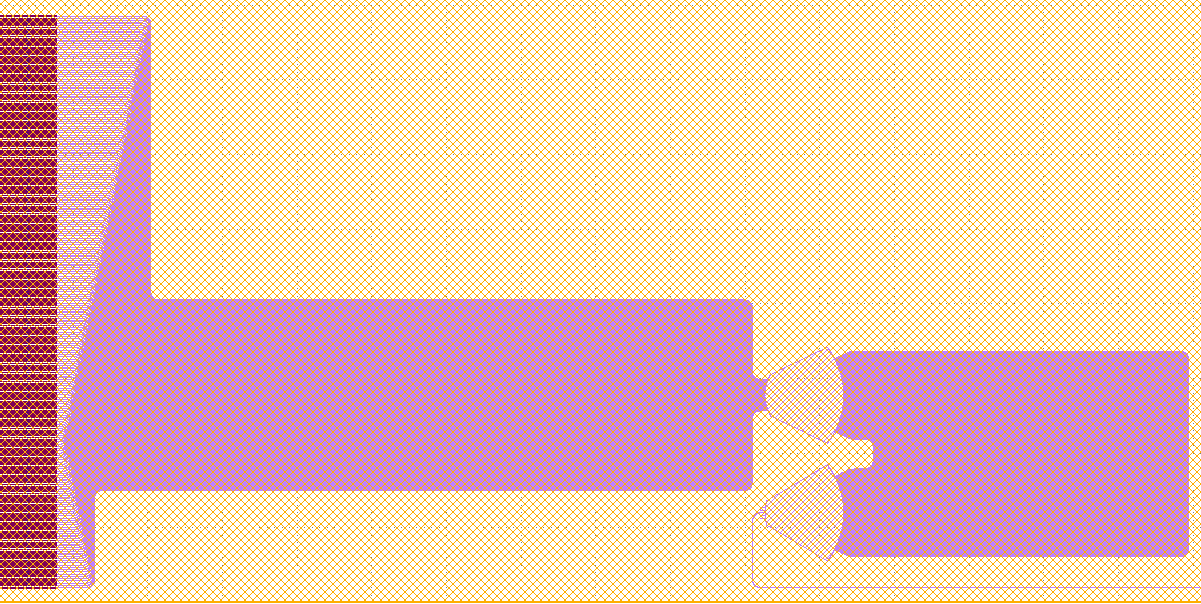
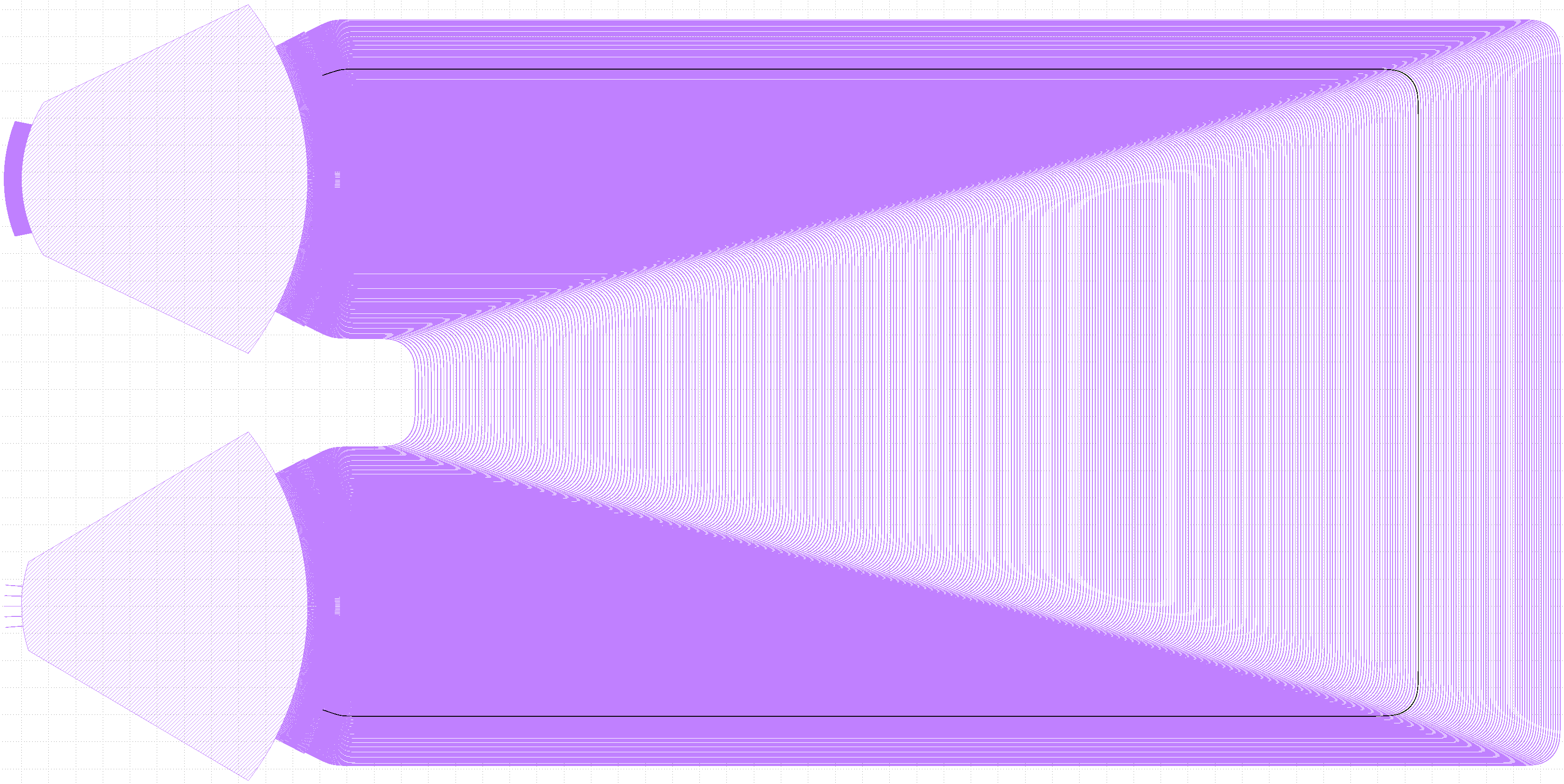
We show here the layout of the generated AWG:
Simulation and analysis
Now that the AWG is assembled, we can use the simulate_awg function to simulate its behaviour.
This function takes the AWG and the wavelengths it simulates as inputs and returns an S-matrix.
# Simulate AWG function
def simulate_awg(awg, wavelengths, save_dir=None, tag=""):
    """

    Parameters
    ----------
    awg: i3.PCell
        Input AWG cell
    wavelengths:
        Wavelengths for the simulation.
    save_dir : str, optional, default: None
        If specified, a .z file is saved in this directory
    tag: str, optional, default: ""
        String used to give a name to saved files

    Returns
    -------

    """
    oct_awg_cm = awg.get_default_view(i3.CircuitModelView)
    print("Simulating AWG...\n")
    awg_s = oct_awg_cm.get_smatrix(wavelengths)
    if save_dir:
        smatrix_path = os.path.join(save_dir, f"smatrix_{tag}.s{awg_s.data.shape[0]}p")
        awg_s.to_touchstone(smatrix_path)
        print(f"{smatrix_path} written")
    return awg_s
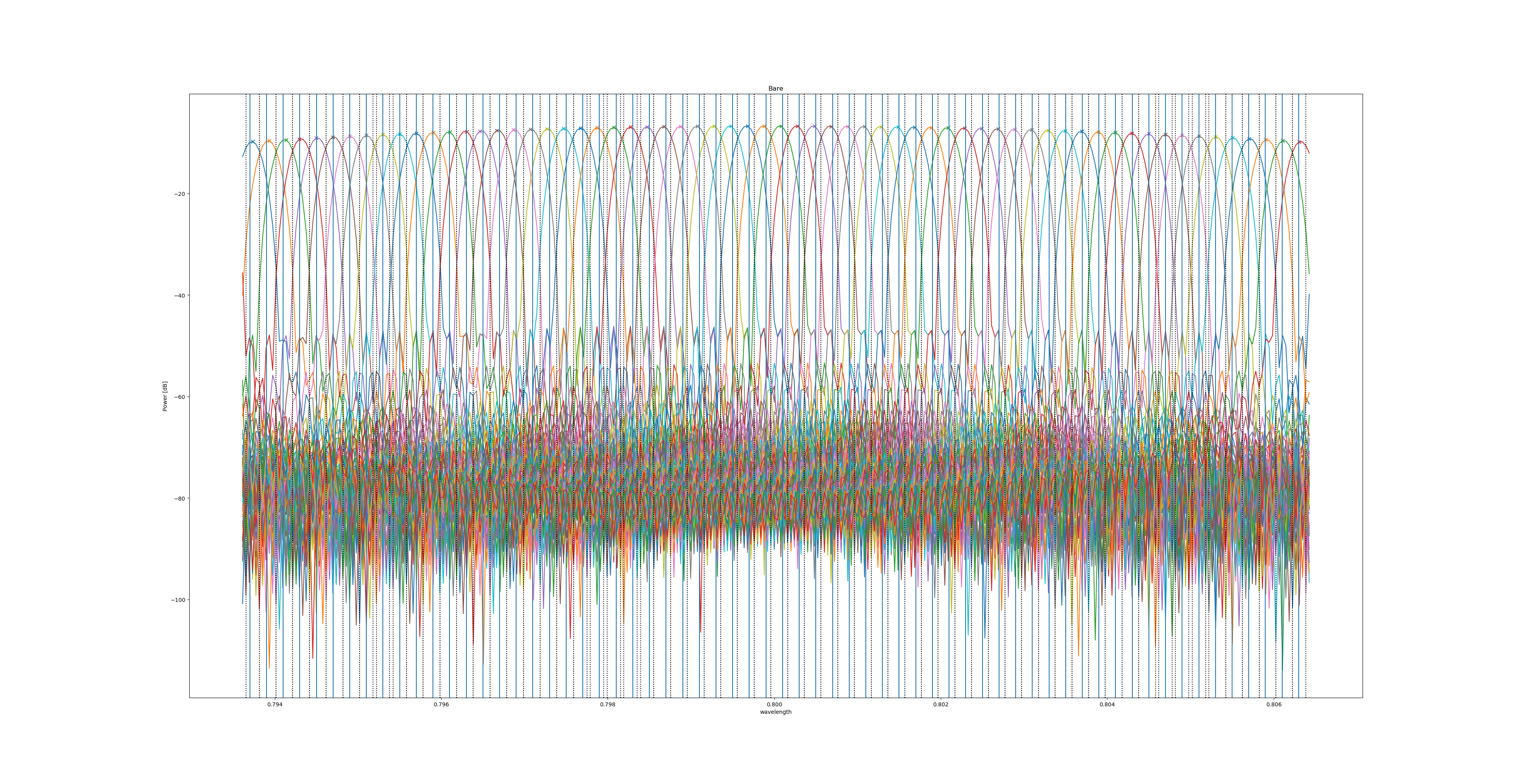
The analyze_awg function then takes this S-matrix together with the parametric specifications of the AWG (center_wavelength, fsr_wavelength and n_channels) in order to calculate a number of figures of merit, that are written to a file, before plotting its simulation results.
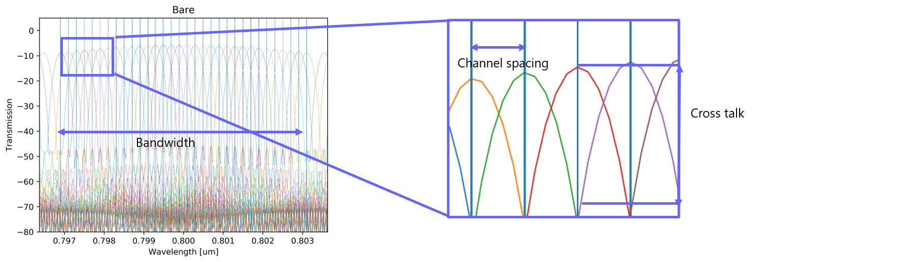
These figures of merit are the error in the peak wavelengths compared to the channel positions, the insertion loss and the level of crosstalk.
The crosstalk provides a limiting factor to the imaging depth [5].
We show the code for this function below.
# Analyze AWG function
def analyze_awg(
    awg_s,
    center_wavelength,
    channel_spacing,
    n_channels,
    peak_threshold=-20.0,
    plot=True,
    save_dir=None,
    tag="",
):
    """Custom AWG analysis function for a spline AWG

    Parameters
    ----------
    awg_s: SMatrix1DSweep
        S-matrix of the AWG
    center_wavelength: float
        Center wavelength of the AWG
    channel_spacing: float
        channel spacing of the AWG.
    n_channels: int
        Number of channels of the AWG
    peak_threshold: float, default: -20.0, optional
        The power threshold for peak detection  (in dB)
    plot: bool, default: True
        If true the spectrum  is plotted
    save_dir: str, optional, default: None
        If specified, a GDSII file is saved in this directory
    tag: str, optional, default: ""
         String used to give a name to saved files

    Returns
    ------
    report: dict
        Dictionary containing analysis specs
    """

    # Specs
    sim_wav = awg_s.sweep_parameter_values
    channel_wavelengths = np.array(
        [center_wavelength + (cnt - (n_channels - 1) / 2.0) * channel_spacing for cnt in range(n_channels)]
    )
    channel_numbers = np.arange(len(channel_wavelengths))
    in_window = (channel_wavelengths > sim_wav[0]) & (channel_wavelengths < sim_wav[-1])
    channel_wav = channel_wavelengths[in_window]
    channel_numbers = channel_numbers[in_window]
    channel_width = 1e-4
    output_ports = [f"out{p + 1}" for p in channel_numbers]

    # Initialize spectrum analyzer
    analyzer = i3.SpectrumAnalyzer(
        smatrix=awg_s,
        input_port_mode="in1:0",
        output_port_modes=output_ports,
        dB=True,
        peak_threshold=peak_threshold,
    )
    analyzer = analyzer.trim(
        (
            min(channel_wav) - channel_width,
            max(channel_wav) + channel_width,
        )
    )

    # Measurements
    peaks = analyzer.peaks()
    peak_wavelengths = [peak["wavelength"][0] for peak in peaks.values()]
    peak_error = np.abs(channel_wav - peak_wavelengths)

    bands = analyzer.width_passbands(channel_width)
    insertion_loss = list(analyzer.min_insertion_losses(bands=bands).values())
    cross_talk_near = list(analyzer.near_crosstalk(bands=bands).values())
    cross_talk_far = list(analyzer.far_crosstalk(bands=bands).values())
    passbands_3dB = list(analyzer.cutoff_passbands(cutoff=-3.0).values())

    # Create report
    report = dict()
    band_values = list(bands.values())
    for cnt, port in enumerate(output_ports):
        channel_report = {
            "peak_expected": channel_wav[cnt],
            "peak_simulated": peak_wavelengths[cnt],
            "peak_error": peak_error[cnt],
            "band": band_values[cnt][0],
            "insertion_loss": insertion_loss[cnt][0],
            "cross_talk": cross_talk_far[cnt] - insertion_loss[cnt][0],
            "cross_talk_nn": cross_talk_near[cnt] - insertion_loss[cnt][0],
            "passbands_3dB": passbands_3dB[cnt][0],
        }
        report[port] = channel_report

    if save_dir:

        def serialize_ndarray(obj):
            return obj.tolist() if isinstance(obj, np.ndarray) else obj

        report_path = os.path.join(save_dir, f"report_{tag}.json")
        with open(report_path, "w") as f:
            json.dump(report, f, sort_keys=True, default=serialize_ndarray, indent=0)
        print(f"{report_path} written")

    # Plot spectrum and specified channels
    fig = analyzer.visualize(title=tag.capitalize(), show=False)
    for spec_wavelength in channel_wav:
        plt.axvline(x=spec_wavelength)

    for passband in passbands_3dB:
        plt.axvline(x=passband[0][0], color="k", linestyle=":")
        plt.axvline(x=passband[0][1], color="k", linestyle=":")

    png_path = os.path.join(save_dir, f"spectrum_{tag}.png")
    fig.savefig(os.path.join(save_dir, png_path), bbox_inches="tight")
    print(f"{png_path} written")

    if plot:
        # Plot transmission spectrum
        plt.show()
    plt.close(fig)
    return report
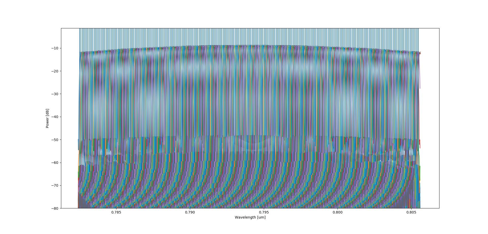
These figures of merit are written to a json file in the same directory used to store the GDS files, design parameters and simulation results. Information on the cross-talk can be found in the entries ‘cross_talk’ and ‘cross_talk_nn’ for each output channel. The latter provides the highest cross-talk between each channel and its nearest neighbors. The former provides the highest cross-talk each channel has with any other channel, excluding its nearest neighbors. We show the simulation results together with both the found and expected peaks below:
All of simulate_awg and most of analyze_awg are identical to that used in the AWG demultiplexer tutorial.
For full documentation refer to the page AWG simulation and analysis.
Finalization
Finally, in our last step, we finalize the AWG by fixing a common design rule violation (acute angles) and routing it.
We fix these violations only in the star couplers in order to save time when we run this code for very large AWGs.
We route the AWG to edge couplers implemented in the AN150BB_EdgeCoupler_Lensed_C PCell in the Ligentec PDK.
We place this all on a large (10 mm x 5 mm) Ligentec frame.
We place the code for doing this in finalize_awg.
# Finalize AWG function
def finalize_awg(awg, save_dir=None, tag="", write_gds=True):
    """Custom function to finalize an AWG design, mostly for DRC fixing and routing.
    If you make an AWG, you should write one of your own.
    Parameters are the things you want to vary as well as options to control whether you save your data.

    Parameters
    ----------
    awg: i3.PCell
        Input AWG cell
    save_dir : str, optional
        If specified, a GDSII file is saved in this directory
    tag: str, optional
        String used to give a name to saved files
    write_gds: bool, default: True
        If True, a GDSII containing the layout of the AWG is exported.

    Returns
    -------
    awg_block: i3.PCell
        Finalized AWG block
    """

    # Fix design rule violations
    # Two types of violations may occur in the AWG: acute (sharp) angles and snapping errors.
    # We use get_stub_elements and flat_copy to fix these.
    print("Fixing design rule violations...")
    print(
        "You can expect warnings below regarding routes in the fanout of the AWG.\n"
        "The reason is that the AWG design allows tighter spacing for the routes connecting "
        "its outputs to the edge couplers.\n"
    )
    awg_layout = awg.get_default_view(i3.LayoutView)
    awg_netlist = awg.get_default_view(i3.NetlistView)
    awg_circuit = awg.get_default_view(i3.CircuitModelView)

    # We look for acute angles in the X1P layer in the awg,
    # typically caused by two apertures that are close together.
    elems_add, elems_subt = i3.get_stub_elements(
        layout=awg_layout,
        angle_threshold=0,
        layers=[i3.TECH.PPLAYER.X1P],
        grow_amount=0.001,
    )

    # Wrap in a cell with a clean layout
    flat_layout = awg_layout.layout.flat_copy() + elems_add
    awg_clean = i3.EmptyCell(name="awg_clean")
    awg_clean.Layout(layout=flat_layout, ports=awg_layout.ports)
    awg_clean.Netlist(terms=awg_netlist.terms)
    awg_clean.CircuitModel(model=awg_circuit.model)

    top_cell = RoutedAWG(
        dut=awg_clean,
        out_dy=25.0,
        bend_radius=50.0,
    )
    top_cell_layout = top_cell.Layout()

    if save_dir and write_gds:
        gds_path = os.path.abspath(os.path.join(save_dir, f"{tag}.gds"))
        top_cell_layout.write_gdsii(gds_path)
        print(f"{gds_path} written.")

    return top_cell
This code calls the class ‘’RoutedAWG’’, which we define so as to route the waveguides to the edge couplers:
# Route the AWG
class RoutedAWG(i3.Circuit):
    dut = i3.ChildCellProperty()
    out_dy = i3.NonNegativeNumberProperty(default=25.0)
    out_y0 = i3.NonNegativeNumberProperty(allow_none=True)
    bend_radius = i3.PositiveNumberProperty(default=50.0)
    wav_spacing = i3.NonNegativeNumberProperty(default=5.0)

    def _default_specs(self):
        awg_ports = self.dut.get_default_view(i3.LayoutView).ports
        tt = awg_ports[0].trace_template.cell
        # To extend the port of AN150BB_EdgeCoupler_Lensed_C to the edge
        extended_taper = ExtendPorts(
            contents=pdk.AN150BB_EdgeCoupler_Lensed_C(),
            port_labels=["in0"],
        )
        extended_taper.Layout(
            extension_length=10.0,
            flatten_contents=False,
        )
        # Adding Taper as the transition
        taper = AutoTransitionPorts(
            contents=extended_taper,
            port_labels=["in0"],
            trace_template=tt,
        )

        frame = pdk.LigentecLarge()

        specs = [
            i3.Inst([f"t{p.name}" for p in awg_ports], taper),
            i3.Inst("DUT", self.dut),
            i3.Inst("frame", frame),
        ]

        # placement
        awg_out_ports = [p for p in awg_ports.y_sorted() if "out" in p.name]
        frame_layout = frame.get_default_view(i3.LayoutView)

        x_dut, y_dut = 5100, 600
        specs += [i3.Place("DUT:in1", (x_dut, y_dut))]

        y_m = y_dut + np.mean([p.position.y for p in awg_out_ports])
        if self.out_y0 is None:
            # Align the center of the tapers with the center of the AWG outputs
            out_y0 = y_m - (len(awg_out_ports) - 1) * self.out_dy / 2.0
        else:
            out_y0 = self.out_y0
        specs.extend(
            [
                i3.Place(
                    f"t{p.name}:out0",
                    (frame_layout.size_info().west + 10, out_y0 + cnt * self.out_dy),
                    180.0,
                )
                for cnt, p in enumerate(awg_out_ports)
            ]
        )

        specs.append(i3.Place("tin1:out0", (frame_layout.size_info().east - 10, 100), 0.0))

        # routing
        out_ports = [f"DUT:{p.name}" for p in awg_out_ports]
        taper_ports = [f"t{p.name}:in0" for p in awg_out_ports]
        specs.append(
            i3.ConnectManhattan(
                "tin1:in0",
                "DUT:in1",
                bend_radius=self.bend_radius,
                min_straight=0.0,
            )
        )

        specs.append(
            i3.ConnectManhattanBundle(
                connections=list(zip(taper_ports, out_ports)),
                start_fanout=i3.SBendFanout(end_position=(700, y_m)),
                end_fanout=i3.SBendFanout(end_position=(4800, y_m)),
                bend_radius=self.bend_radius,
                pitch=self.wav_spacing,
                min_spacing=3.0,
                name="bundle",
            )
        )
        return specs

    def _default_exposed_ports(self):
        awg_ports = self.dut.get_default_view(i3.LayoutView).ports
        return {f"t{p.name}:out0": p.name for p in awg_ports}


# Finalize AWG function
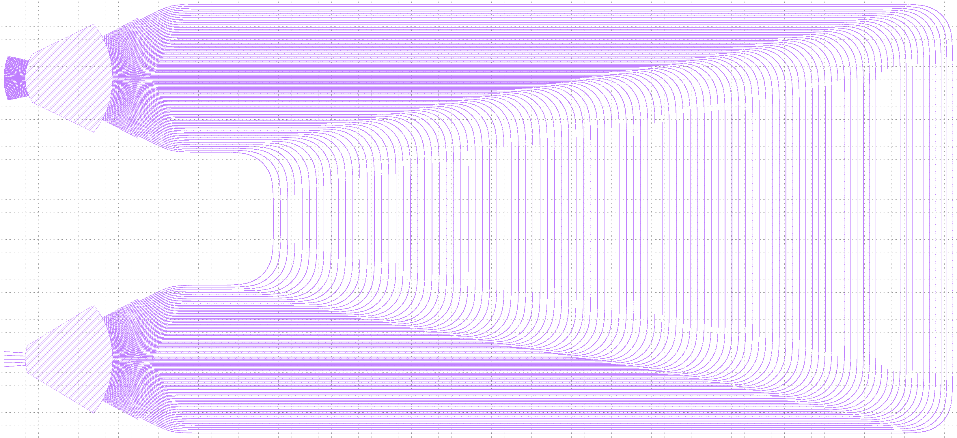
Here are the finalized layout and output spectrum of the AWG.
Test your knowledge
When designing an AWG for OCT, there are a number of trade-offs that need to be considered. In this section, we invite you to explore these trade-offs as part of the exercises.
Exercise 1 - channel spacing vs crosstalk
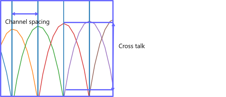
Let’s design our AWG in such a way as to maximize the imaging depth. As we previously mentioned, the imaging depth increases as we reduce the channel spacing and also when we reduce the crosstalk. However, reducing the channel spacing has the effect of increasing the crosstalk. This leads to their being a trade-off between the channel spacing and the crosstalk when seeking to maximize the imaging depth.
Try reducing the channel spacing of the AWG, keeping the number of channels constant. In this training material, you can find information on the crosstalk in the file named oct_awg_X_Y/report_finalized.json where X is the wavelength and Y is the FSR. You can also estimate it by looking on the graph of the simulation result. In this case, the value you want is the nearest neighbour crosstalk which is the value “cross_talk_nn” which is calculated for each channel.
Explore what happens when you reduce the channel spacing. How much does the nearest neighbour crosstalk (for a specific channel you choose) increase?
Exercise 2 - Crosstalk vs footprint vs insertion loss
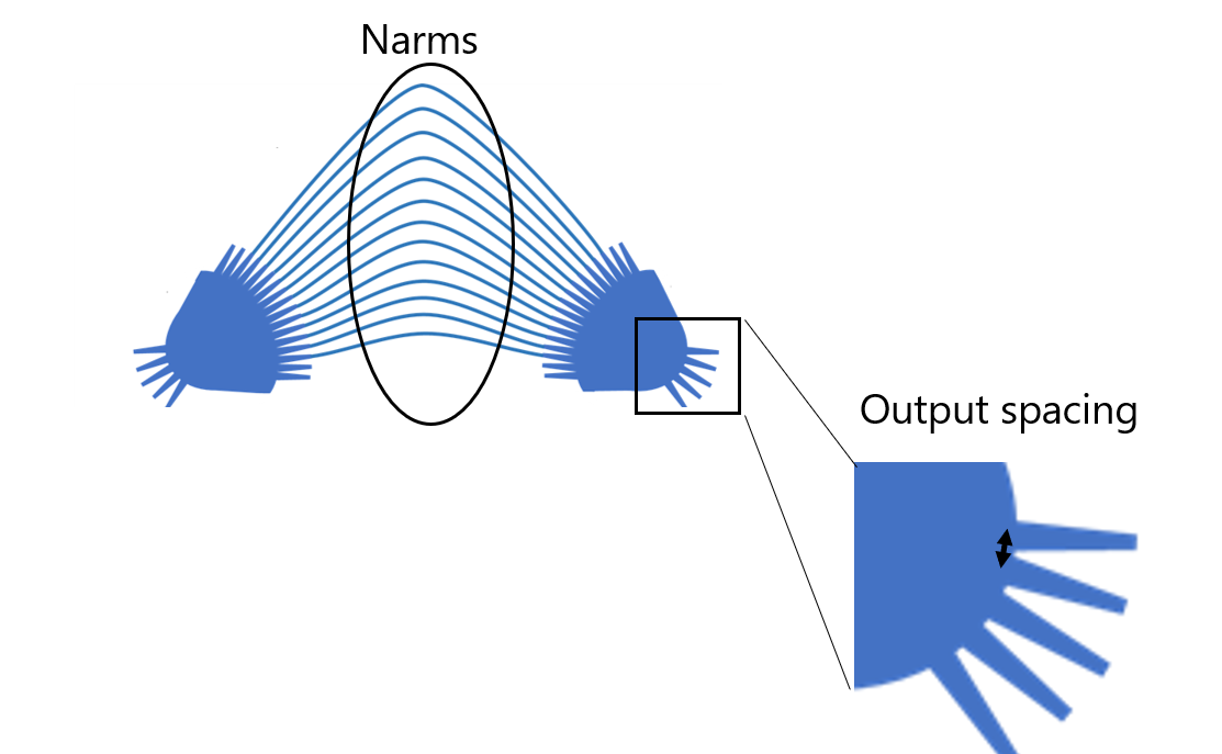
Try varying the number of arms of the AWG.
As expected, you will find that the footprint of the AWG increases with the number of arms. However, you will find that the crosstalk of the AWG decreases with it as well. How do you have to increase the number of arms to achieve of at least 10 dB in the crosstalk? How much does the footprint increase?
Try varying the output spacing of the AWG.
As expected, you will find that the footprint of the AWG increases a bit However, you will find that the crosstalk of the AWG decreases with it while the insertion loss increases What is the output spacing to achieve of at least 10 dB in the crosstalk? What is the insertion loss then?
Exercise 3 - Number of output channels vs footprint
To optimize for both the imaging depth and the axial resolution, you must increase the number of output channels.
Now, set once again n_arms = None to make the number of arms automatic.
See what happens if you increase the number of output channels.
How much does the footprint increase with 100 output channels compared to 64?
In your own time, try to achieve the same parameters as in the OCT paper [1] with 256 output channels, a center wavelength of 794 nm, a wavelength spacing of 0.09 nm and a bandwidth of 22 nm. Note that it may take some time to generate and simulate such a large AWG. Once fully routed, you should be able to see the following layout for this AWG with the following output spectrum: