Optical phased array (OPA)
Integrated optical phased arrays (OPAs) enable beam steering at low cost compared to bulk optics systems. They are used in many applications including:
Sensing
Imaging
Displays
Light Detection and Ranging (LiDAR)
Telecommunications, such as demultiplexing switches
The Luceda Photonics Design Platform is very well suited for the design and simulation of OPAs because it allows simultaneous parametric control of both the layout and the simulation of integrated photonic circuits using a scripting approach. As OPAs are large - yet regular - circuits, this approach allows the designer to scale simple design concepts to large designs that are easy to simulate while being confident that the simulations match the layout.
In this application example we will show how to create this parametric control in both layout and simulation for the design of an OPA. The methodology used here can be easily applied to circuits that have similar requirements, such as switch arrays, optical computing arrays or quantum computing arrays.
Our main focus will be on the file structure and the coding style so that this approach can be applied easily to many different circuits.
Introduction
An optical phased array consists of a splitter tree whose every output is connected to a heater. If you would like to learn how to design a splitter tree using Luceda IPKISS, we recommend that you have a look at Designing a splitter tree before continuing with this tutorial. In addition, in Thermo-optic phase shifter (Heater) you may find an explanation on how to design and simulate a heater.
In this application example, we will go through the following steps:
First, we instantiate and simulate a pre-defined unrouted OPA (
OPA). This way, we get a first feeling of what the final goal is in terms of layout and simulation.Next, we dig deeper into the code of the
OPAPCell.We analyze how the simulation recipe of the OPA is defined.
Finally, we route the OPA to grating couplers and bond pads, obtaining the
RoutedOPAPCell. We instantiate the routed OPA and simulate it.
Unrouted OPA: visualization and simulation
We have designed an OPA PCell, called OPA and we have stored it in opa/cell.py.
This PCell is unrouted which means that it has not yet been connected to contact pads and grating couplers.
We are now going to use this PCell in example_unrouted_opa.py to instantiate an OPA and simulate it.
Instantiating the parametric components of the OPA
Many circuits, including the OPA we have designed in opa/cell.py, contain components that the designer may want to vary.
In this case, we have chosen the heater PCell to be a property of the OPA.
This allows for maximum flexibility, as the designer may decide at a later moment to use a different heater without needing to define a new PCell for the OPA.
Therefore, the first step towards creating the OPA is to instantiate the heater PCell with the desired length.
# Heater
heater = pdk.HeatedWaveguide(name="heated_wav")
heater.Layout(shape=[(0, 0), (1000.0, 0.0)])
Instantiating the unrouted OPA
Next, we instantiate the unrouted OPA PCell (OPA) which has the following properties:
heater: Heater PCell used in the OPA, at the outputs of the splitter tree.splitter: Splitter PCell used in the OPA, in the splitter tree.levels: Number of levels in the splitter tree.spacing_y: Horizontal spacing between the levels of the splitter tree.spacing_x: Vertical spacing between the splitters in the last level.
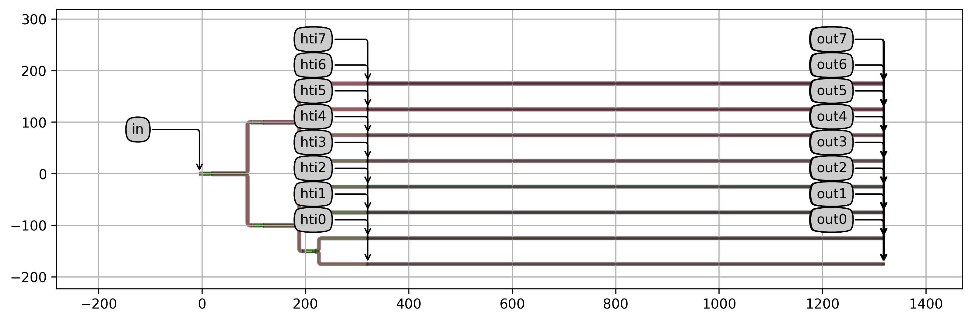
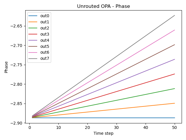
The resulting circuit has a layout that can be visualized:
# Unrouted OPA
opa = OPA(name="opa_array", heater=heater, levels=3)
opa_lv = opa.Layout()
opa_lv.visualize(annotate=False)
It also has a circuit model that can be simulated using the simulate_opa function (pre-defined in opa/simulate.py) which defines the simulation recipe of the OPA.
# Simulation
res = simulate_opa(cell=opa)

plt.figure()
for cnt in range(opa._get_n_outputs()):
    plt.plot(res.timesteps[1:], np.unwrap(np.angle(res[f"out{cnt}"]))[1:], label=f"out{cnt}")

plt.title("Unrouted OPA - Phase")
plt.xlabel("Time step")
plt.ylabel("Phase")
plt.legend()
plt.tight_layout()
plt.show()
Unrouted OPA: parametric cell
Now, we are ready to dig deeper into the IPKISS code that defines the unrouted OPA PCell.
class OPA(i3.Circuit):
    """Class for an optical phased array (OPA) composed of a splitter tree and an array of heaters."""

    _name_prefix = "OPA"

    heater = i3.ChildCellProperty(doc="Heater PCell used at the outputs of the splitter tree")
    splitter = i3.ChildCellProperty(doc="Splitter PCell used in the splitter tree")
    levels = i3.PositiveIntProperty(default=4, doc="Number of levels in the splitter tree")
    spacing_y = i3.PositiveNumberProperty(
        default=50.0,
        doc="Vertical spacing between the levels of the splitter tree",
    )
    spacing_x = i3.PositiveNumberProperty(
        default=100.0,
        doc="Horizontal spacing between the splitters in the last level",
    )

    def _get_n_outputs(self):
        return 2**self.levels

    def _default_heater(self):
        # By default, the heater is a 1 mm-long heated waveguide
        ht = pdk.HeatedWaveguide()
        ht.Layout(shape=[(0.0, 0.0), (1000.0, 0.0)])
        return ht

    def _default_splitter(self):
        return pdk.MMI1x2Optimized1550()

    def _default_specs(self):
        # Create a splitter tree, then add a heater at each output

        splitter_tree = pteam_lib.SplitterTree(
            levels=self.levels,
            splitter=self.splitter,
            spacing_y=2 * self.spacing_y,
        )
        specs = [
            i3.Inst("tree", splitter_tree),
            i3.Inst([f"ht{cnt}" for cnt in range(self._get_n_outputs())], self.heater),
        ]
        # Position the heaters and connect them to the splitter tree
        east = splitter_tree.get_default_view(i3.LayoutView).size_info().east
        n_outputs = self._get_n_outputs()
        for n_out in range(n_outputs):
            specs += [
                i3.Place(
                    f"ht{n_out}",
                    (east + self.spacing_x, (n_out - (n_outputs - 1) / 2.0) * self.spacing_y),
                ),
                i3.ConnectManhattan(
                    f"ht{n_out}:in",
                    f"tree:out{n_out + 1}",
                ),
            ]
        return specs

    def _default_exposed_ports(self):
        # Set the names of the electrical ports
        exposed_ports = dict()
        exposed_ports["tree:in"] = "in"
        for n_out in range(self._get_n_outputs()):
            exposed_ports[f"ht{n_out}:elec1"] = f"hti{n_out}"
            exposed_ports[f"ht{n_out}:elec2"] = f"hto{n_out}"
            exposed_ports[f"ht{n_out}:out"] = f"out{n_out}"
        return exposed_ports
Let’s take a closer look:
The
OPAPCell inherits fromi3.Circuitin order to create the circuit.The heater used at the outputs of the splitter tree is a property of the OPA (
heater). Therefore, it can be parametrically changed when the OPA is instantiated as we have already done in the previous step.We use a splitter tree from P-Team library (based on SiFab). Note that here the parametricity of
SplitterTreehere is handy as we can change both the spacing and the splitter PCell according to the requirements of the OPA we want to design.All components are placed using the functionality offered by
i3.Circuit.All the input and output electrical ports of the heaters are propagated to the next level.
Ports are renamed to a shorter name for easier handling.
Simulation recipe
The goal of a simulation recipe is to find out what is the performance of a device or circuit. Inside the simulation recipe, we script the interactions with the simulators that are required to answer that question.
For the OPA the questions is: what is the phase difference at the end of the array when a voltage sweep is applied across the heater array? To answer this question, we perform an optical circuit simulation in time domain.
Naturally, we want to be able to vary the relevant parameters that affect the behaviour of the OPA. Therefore, we create a parametric simulation recipe. In our case the parameters are:
cell: OPA PCell to be simulateddv_start: Linear difference in voltage at the beginning of the sweepdv_end: Linear difference in voltage at the end of the sweepnsteps: Number of steps to be used in the voltage sweepcenter_wavelength: Center wavelengthdebug: If True, the simulation is run in debug mode
The simulate_opa function takes these parameters as input and returns the time response at the output of our circuit.
from math import sqrt
from ipkiss3 import all as i3
import re


def simulate_opa(
    cell,
    dv_start=0.0,
    dv_end=1.0,
    nsteps=50,
    center_wavelength=1.5,
    debug=False,
):
    """Simulation recipe to simulate an optical phased array (OPA) by sweeping the bias voltage.

    Parameters
    ----------
    cell : i3.PCell
        OPA PCell to be simulated
    dv_start : float
        Linear difference in voltage at the beginning of the sweep
    dv_end : float
        Linear difference in voltage at the end of the sweep
    nsteps : int
        Number of steps to be used in the voltage sweep
    center_wavelength : float
        Center wavelength
    debug : bool
        If True, the simulation is run in debug mode

    Returns
    -------
    Time response

    """
    dt = 1
    t0 = 0
    t1 = nsteps

    # Get the number of output ports
    dut_lv = cell.get_default_view(i3.LayoutView)
    port_list_out_sorted = [p.name for p in dut_lv.ports.y_sorted() if re.search("(out)", p.name)]
    n_outs = len(port_list_out_sorted)

    # Define the optical source at the input.
    # Note, FunctionExcitation is a PCell.
    # It's essentially a component that is placed in the circuit and sends a signal into the chip
    # through its output port.
    #
    # Using the argument port_domain, you can specify whether to input an optical or electrical signal,
    # excitation_function provides the input signal in terms of time.

    optical_in = i3.FunctionExcitation(
        port_domain=i3.OpticalDomain,
        excitation_function=lambda t: 1.0,
    )

    # Use nested functions to generate a function that defines the distribution
    # of the electrical signal, in volts, in terms of time.
    def get_source(v_start, v_end):
        def linear_ramp(t):
            # The phase shift is a quadratic function of the voltage, so to get a linear ramp of the phase
            # the voltage follows a non-linear square root ramp.
            return v_end * (t / t1) ** 0.5 + v_start * ((t1 - t) / t1) ** 0.5

        return linear_ramp

    # Define the child cells and links (direct connections)
    child_cells = {
        "DUT": cell,
        "optical_in": optical_in,
    }
    links = [("optical_in:out", "DUT:in")]

    for cnt in range(n_outs):
        # Define sources of electrical signals at electrical ports
        child_cells[f"v{cnt}"] = i3.FunctionExcitation(
            port_domain=i3.ElectricalDomain,
            # The phase changes quadratic in function of the applied voltage,
            # so to get the same phase difference between all outputs we use square root increments.
            excitation_function=get_source(sqrt(cnt) * dv_start, sqrt(cnt) * dv_end),
        )
        links.append((f"v{cnt}:out", f"DUT:hti{cnt}"))

        child_cells[f"out{cnt}"] = i3.Probe(port_domain=i3.OpticalDomain)
        links.append((f"out{cnt}:in", f"DUT:out{cnt}"))

    # Create a test bench by connecting the sources to the ports of the circuit using ConnectComponent
    testbench = i3.ConnectComponents(
        child_cells=child_cells,
        links=links,
    )

    # Now we simulate the test bench and return the time response.
    print(f"Simulating circuit between {t0} and {t1} with step {dt} - nsteps {nsteps}")

    cm = testbench.CircuitModel()
    results = cm.get_time_response(
        t0=t0,
        t1=t1,
        dt=dt,
        center_wavelength=center_wavelength,
        debug=debug,
    )

    return results
Routed OPA: parametric cell
As a final step, we create the RoutedOPA PCell (defined in opa/cell.py) that routes an unrouted OPA (such as the one we just created) to the outside world.
The parameters of this PCell are:
DUT: The device under test (DUT), such as the OPA in this example. Note that the code has been written in such a way that it can be generalised to other PCells with electrical ports.bond_pads_spacing: The horizontal distance between the contact pads.wire_spacing: The spacing between the electrical wires.
class RoutedOPA(i3.PCell):
    """Optical phased array (OPA) whose heaters are electrically connected to metal contact pads via electrical wires.
    In this example, the device under test (DUT) is the OPA, but the code has been written in such a way that
    it can be generalised to other PCells with electrical ports.
    """

    # 1. We define the properties of the PCell.
    dut = i3.ChildCellProperty(doc="The device under test, in this case the OPA")
    fgc = i3.ChildCellProperty(doc="Fiber grating couplers PCell")
    bondpad = i3.ChildCellProperty(doc="Bondpads PCell")
    bond_pads_spacing = i3.PositiveNumberProperty(default=100.0, doc="The horizontal distance between the contact pads")
    wire_spacing = i3.PositiveNumberProperty(default=10.0, doc="The spacing between the electrical wires")
    length_of_out_wg = i3.PositiveNumberProperty(default=300.0, doc="Length of output waveguide")
    length_of_in_wg = i3.PositiveNumberProperty(default=300.0, doc="Length of output waveguide")

    def _default_dut(self):
        return OPA(name=self.name + "_opa")

    def _default_fgc(self):
        return pdk.FC_TE_1550()

    def _default_bondpad(self):
        return pdk.BONDPAD_5050()

    class Layout(i3.LayoutView):
        def generate(self, layout):
            # 2. We define the instances that form our circuit.
            # The instances of our circuit are the DUT (the OPA), the grating couplers and the contact pads
            specs = [i3.Inst("DUT", self.dut)]
            dut_lo = self.dut
            for port in dut_lo.ports.optical_ports:
                specs.append(i3.Inst(f"gr_{port}", self.fgc))
            for port in (p for p in dut_lo.ports if p.domain is i3.ElectricalDomain):
                specs.append(i3.Inst(f"bp_{port}", self.bondpad))

            # 3. We define placement and routing specifications.

            # Useful parameters that we will use in our code:
            bp_spacing = self.bond_pads_spacing
            wire_spacing = self.wire_spacing
            bp_height = abs(self.bondpad.size_info().north - self.bondpad.size_info().south)

            # Sorted list of output optical ports of the DUT
            port_list_out_sorted = [p.name for p in dut_lo.east_ports.y_sorted()]

            # Sorted list of electrical ports of the DUT
            el_in_sorted = [p.name for p in dut_lo.ports.y_sorted() if "hti" in p.name]
            el_out_sorted = [p.name for p in dut_lo.ports.y_sorted_backward() if "hto" in p.name]
            n_el_ports = len(el_in_sorted) + len(el_out_sorted)

            # Place the DUT (splitter tree) at the origin
            specs += [i3.Place("DUT", (0, 0))]

            # Place the grating couplers relative to the input and output ports of the DUT
            specs += [i3.Place("gr_in:out", (-self.length_of_in_wg, 0), angle=0.0, relative_to="DUT:in")]
            specs += [
                i3.Place(
                    f"gr_{p}:out",
                    (self.length_of_out_wg, 0),
                    angle=180.0,
                    relative_to=f"DUT:{p}",
                )
                for p in dut_lo.ports
                if "out" in p.name
            ]

            # Place the bondpads
            specs += [
                i3.Place.X(
                    f"bp_{p}:m1",
                    idx * bp_spacing,
                )
                for idx, p in enumerate(el_in_sorted + el_out_sorted)
            ]
            specs += [
                i3.Place.Y(
                    f"bp_{p}:m1",
                    2 * bp_spacing + (n_el_ports // 2) * wire_spacing,
                    relative_to="DUT@N",
                )
                for p in el_in_sorted + el_out_sorted
            ]

            # Connect the output optical ports all to output grating couplers
            specs += [
                i3.ConnectManhattan(
                    f"DUT:{p}",
                    f"gr_{p}:out",
                )
                for p in port_list_out_sorted
            ]

            # Connect the input optical port to the input grating coupler
            specs += [
                i3.ConnectManhattan(
                    "DUT:in",
                    "gr_in:out",
                )
            ]

            # Define trace templates for the electrical routing
            tt = i3.ElectricalWireTemplate()
            tt.Layout(width=4.0, layer=i3.TECH.PPLAYER.M1)

            # Add electrical wiring from the bond pads to the DUT
            top_port_y = max(p.y for p in dut_lo.electrical_ports)
            min_gap = wire_spacing - tt.get_default_view(i3.LayoutView).width
            bend_radius = (min_gap + tt.get_default_view(i3.LayoutView).width) / 2
            pos_v_line = dut_lo.ports[el_in_sorted[-1]].x - bend_radius
            specs.append(
                i3.ConnectElectricalBundle(
                    connections=[(f"DUT:{p}", f"bp_{p}:m1") for p in el_in_sorted],
                    connection_name="DUT_to_bp_m1_in",
                    start_angle=180.0,
                    end_angle=-90.0,
                    end_straight=bp_height,
                    start_straight=0,
                    start_fanout=i3.ManhattanFanout(
                        output_direction=i3.NORTH,
                        reference=f"DUT:{el_in_sorted[-1]}",
                        end_position=(pos_v_line, top_port_y + bend_radius),
                    ),
                    end_fanout=i3.SBendFanout(
                        end_position=(pos_v_line, top_port_y),
                        reference=f"bp_{el_in_sorted[-1]}:m1",
                    ),
                    trace_template=tt,
                    min_gap=min_gap,
                )
            )
            pos_v_line = dut_lo.ports[el_out_sorted[0]].x + bend_radius
            specs.append(
                i3.ConnectElectricalBundle(
                    connections=[(f"DUT:{p}", f"bp_{p}:m1") for p in el_out_sorted],
                    connection_name="DUT_to_bp_m1_out",
                    start_angle=0.0,
                    end_angle=270.0,
                    end_straight=bp_height,
                    start_straight=0,
                    start_fanout=i3.ManhattanFanout(
                        output_direction=i3.NORTH,
                        reference=f"DUT:{el_out_sorted[0]}",
                        end_position=(pos_v_line, top_port_y + bend_radius),
                    ),
                    end_fanout=i3.SBendFanout(
                        end_position=(pos_v_line, top_port_y),
                        reference=f"bp_{el_out_sorted[0]}:m1",
                    ),
                    trace_template=tt,
                    min_gap=min_gap,
                )
            )

            layout = i3.place_and_route(layout=layout, specs=specs)

            exposed_ports = dict()
            exposed_ports["gr_in:vertical_in"] = "in"
            for cnt in range(self.dut.cell._get_n_outputs()):
                exposed_ports[f"gr_out{cnt}:vertical_in"] = f"out{cnt}"
                exposed_ports[f"DUT:hti{cnt}"] = f"hti{cnt}"
                exposed_ports[f"DUT:hto{cnt}"] = f"hto{cnt}"
            layout += i3.expose_ports(
                layout,
                exposed_ports,
                optical="explicit",
                electrical="explicit",
            )
            return layout

    class CircuitModel(i3.CircuitModelView):
        def _generate_model(self):
            return i3.HierarchicalModel.from_netlistview(self.netlist_view)

    class Netlist(i3.NetlistFromLayout):
        pass
Let’s have a closer look at the code:
We inherit directly from
i3.PCellas we will need to manually tune the netlist to include only the electrical parts that we need. Our bond pads and the electrical wires do not have theiri3.CircuitModelViewdefined. We would thus like to remove those entries.We first generate the instances which contain the DUT, all the fiber grating couplers, and bond pads that we need. The number of instances depends on the number of ports our DUT has. This means that the correct number of fiber grating couplers and bond pads is created, depending on the number of optical and electrical outputs in the circuit.
The placement is done using a combination of heuristics to make sure there is enough space for the electrical routing.
We then create the optical connectors. They are based on a sorted list of the optical output ports of the DUT. The idea is that the routing script can detect the number of fiber grating couplers and create connectors for each of them.
Using a similar approach, we define the electrical connectors that create a route between electrical outputs of the heaters and the bond pads. Also, here a sorted list is used.
The whole routing process is performed using connectors and a similar approach to the one used in Fully customized connection bundle for defining the route waypoints.
External port names are exposed and renamed to be the same as in the unrouted OPA. This makes it easier to use the same simulation recipe on both the unrouted and routed circuits as the interface is the same.
Routed OPA: verification, visualization, and simulation
Using the PCell we have just defined (RoutedOPA), we can now instantiate and verify our design.
In example_routed_opa.py, we instantiate the routed OPA, open it IPKISS Canvas, visualize and export to GDSII.
"""Instantiate and simulate a routed optical phased array (OPA).
This script generates several outputs:
- export a schematic to canvas (RoutedOPA.iclib / RoutedOPA.icproject)
- write to GDSII (routed_opa.gds)
- visualize the layout in a matplotlib window (this pauses script execution)
- circuit simulation result (time-domain)
"""
import si_fab.all as pdk
from opa.cell import OPA, RoutedOPA
from opa.simulate import simulate_opa
import matplotlib.pyplot as plt
import numpy as np
tag = "routed_opa"
# Heater
heater = pdk.HeatedWaveguide(name="heated_wav")
heater.Layout(shape=[(0, 0), (1000.0, 0.0)])
# Unrouted OPA
opa = OPA(name="opa_array", heater=heater, levels=3)
# Routed OPA
opa_routed = RoutedOPA(dut=opa, name="RoutedOPA")
opa_routed_lv = opa_routed.Layout()
# Export to IPKISS Canvas for verification.
# When run, previous information (position of symbols, cards, ...) is remembered because the project is stored on disk.
opa_routed_lv.to_canvas()
opa_routed_lv.write_gdsii(f"{tag}.gds")
opa_routed_lv.visualize()
# Simulation
res = simulate_opa(cell=opa_routed)
plt.figure()
for cnt in range(opa._get_n_outputs()):
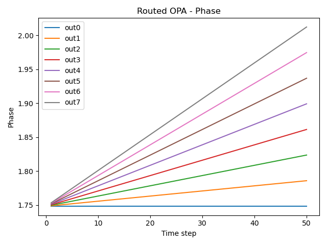
plt.plot(res.timesteps[1:], np.unwrap(np.angle(res[f"out{cnt}"]))[1:], label=f"out{cnt}")
plt.title("Routed OPA - Phase")
plt.xlabel("Time step")
plt.ylabel("Phase")
plt.legend()
plt.tight_layout()
plt.show()
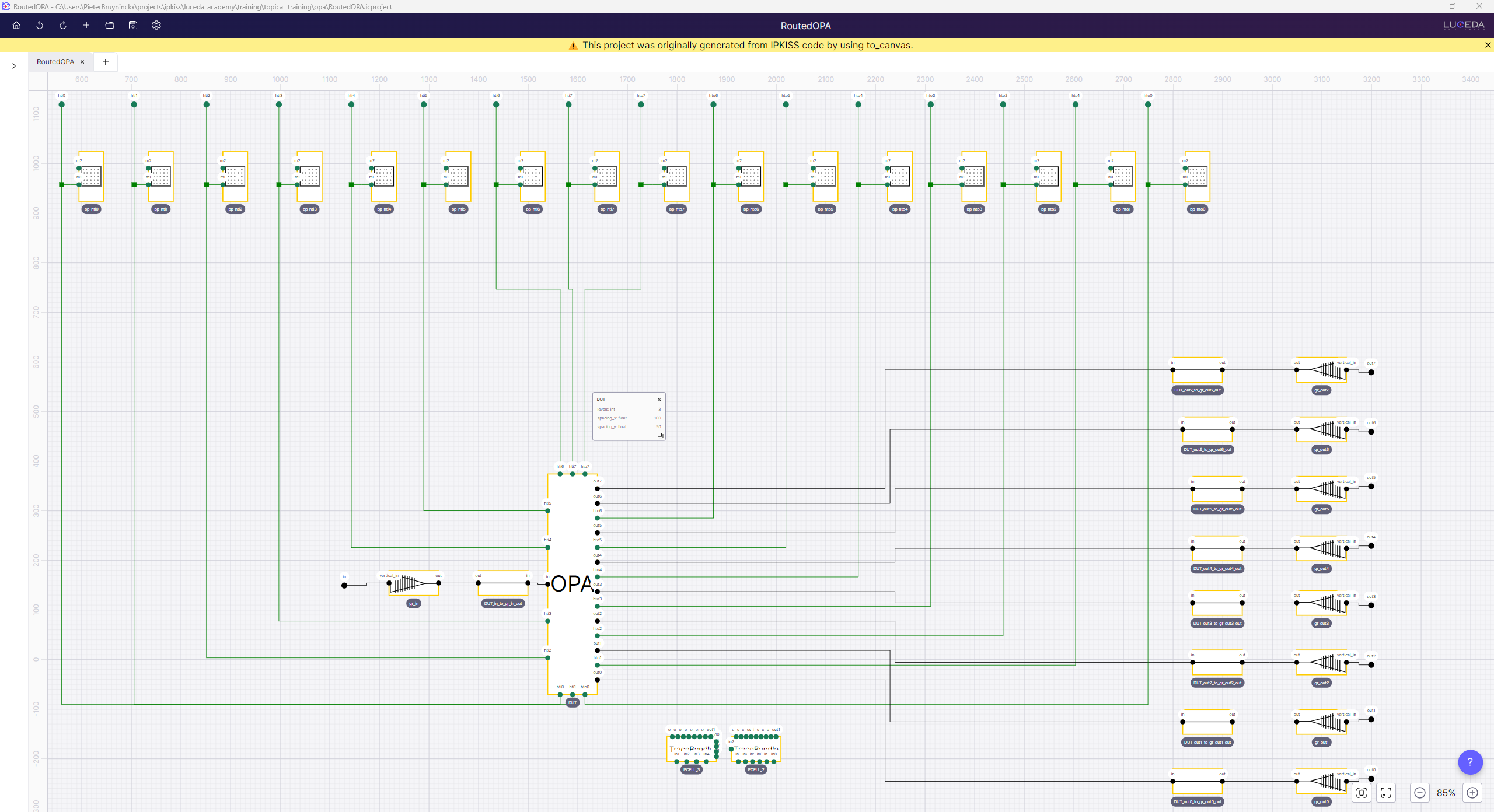
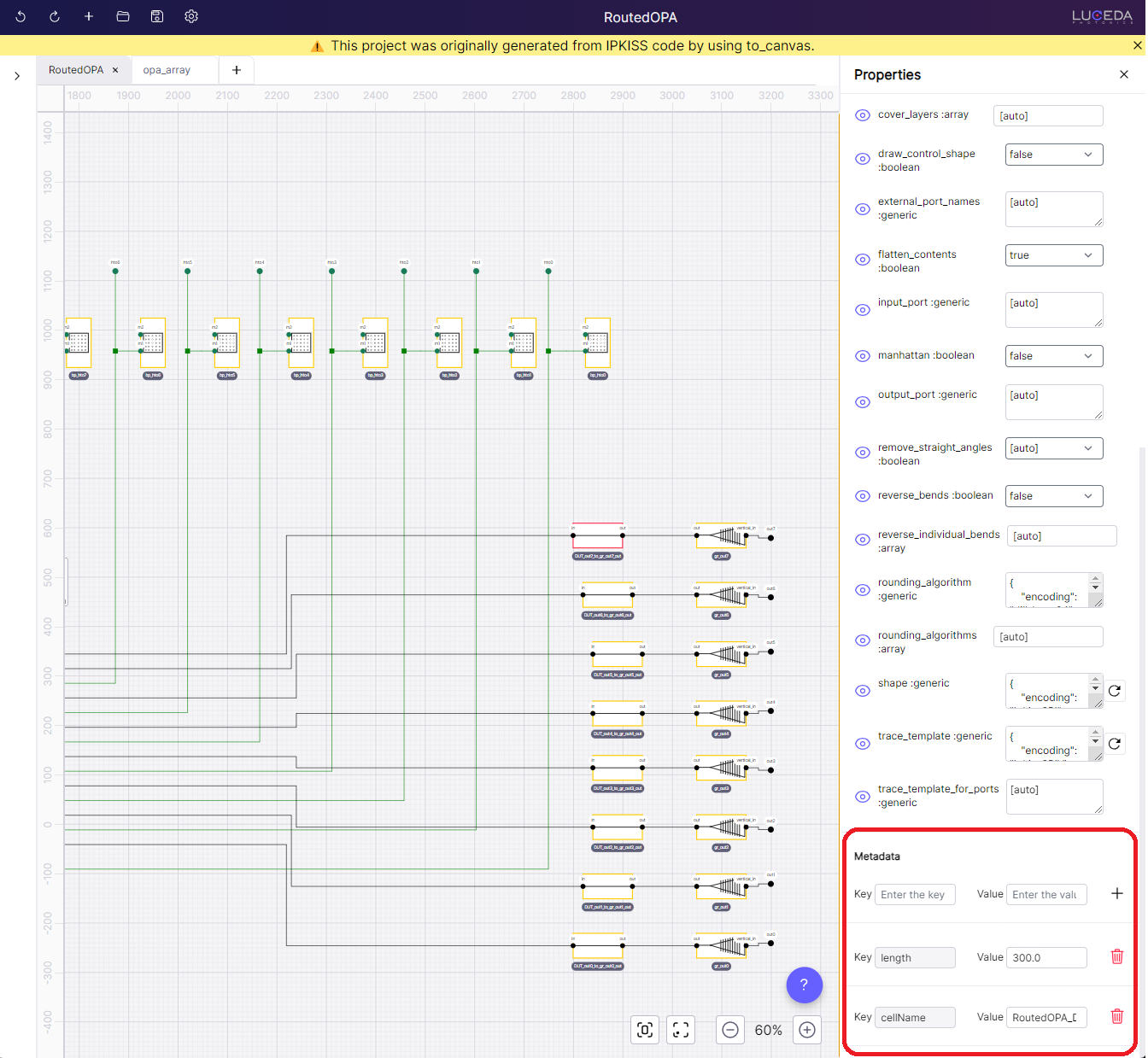
Schematic of routed OPA in IPKISS Canvas generated from layout and after repositioning elements. The banner suggests that this is an auto-generated project.
Let’s have a closer look at the resulting schematic. The banner suggests that this is a project generated from IPKISS Code, as opposed to starting from an clean state (see Schematic capture in IPKISS Canvas). To ensure our circuit is designed as intended, consider these steps:
Confirm Proper Connections: We can verify correct connections exist between instances, by matching them to the specs defined in the
generate(self, layout)method of theRoutedOPAclass. We can also compare the schematic against the visualized layout. You’ll notice two types of nets, electrical ones in green and optical ones in black. Note that the absence of a net might indicate a problem with the connection in the layout. In addition, a group of electrical terms connected together to form a single net could indicate an unintended short circuit.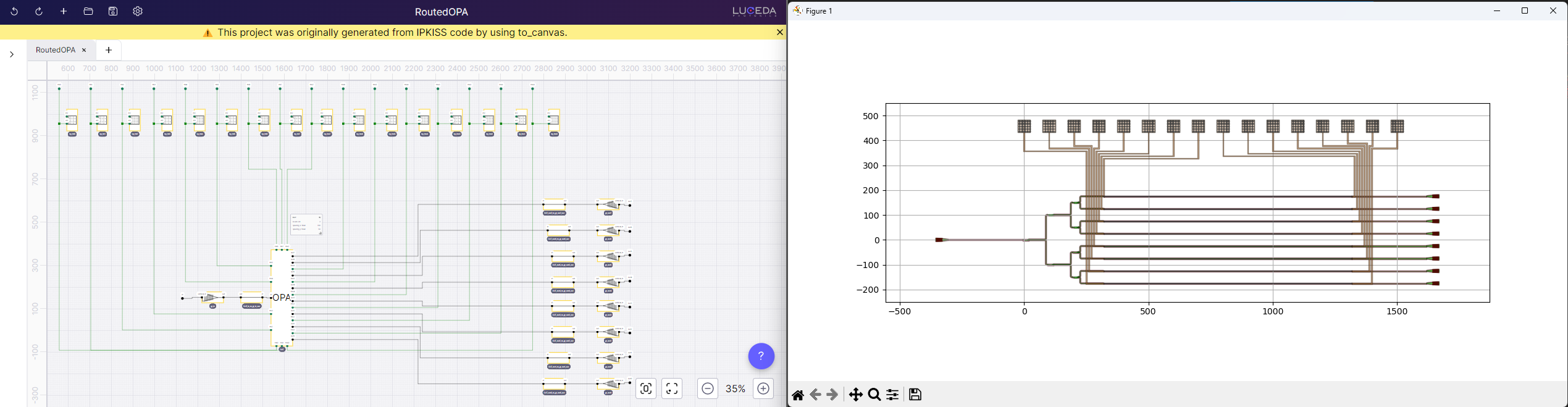
Explore Parameters: The functionality of a particular block depends on the parameters set. To explore those, we can select any of the instances and inspect their properties by opening the context menu (right-click) and selecting
properties. This further displays a pane with various instance parameters exported from the correspondingPCell. Parameters that are different from the default values are marked with a circular arrow. By opening properties of an OPA symbol we can confirm that the parameters are equivalent to the ones set in IPKISS Code. Furthermore, to emphasize the important aspects of our design, we can open cards for each instance, accessible within the symbol instance context menu. Use cards to highlight the critical circuit aspects for easy verification.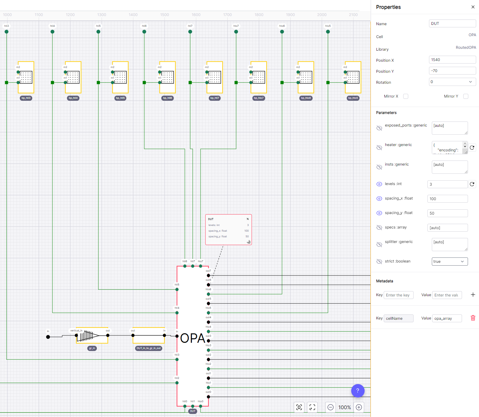
Review Design Requirements: Schematics extracted from IPKISS code include annotations, which let us review some of the designs requirements. We can open properties of the waveguides connecting the OPA to the output grating couplers, to confirm a uniform waveguide length throughout. In addition, annotations can be customized to broaden the way we verify the circuit e.g. by adding loss to the waveguides.
Exploring Hierarchy: Let’s deep dive into the OPA circuit (right-click -> “Open Schematic”). Designs generated with
to_canvasare exported hierarchically. This allows us to explore the resulting sub-circuit schematics and apply the same verification steps as we did with theRoutedOPA.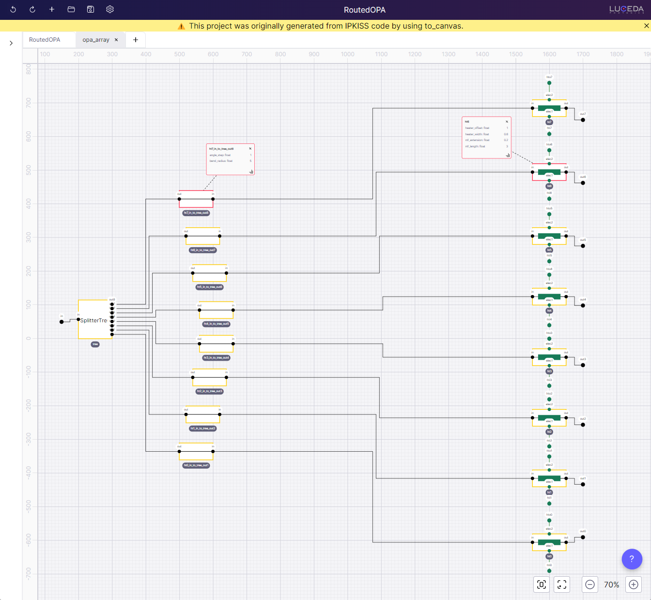
Schematic of OPA after repositioning elements.
The project (RoutedOPA.icproject) can be opened from a file explorer. Changes to the schematics are stored in RoutedOPA.iclib. Manual changes you make inside IPKISS Canvas such as moving instances and displaying cards, will be retained even if you execute to_canvas multiple times.
As the last step, we perform a simulation of the routed OPA.

Conclusion
In this application example, we have seen how to construct a routed optical phase array (OPA) by leveraging the flexibility and parametricity both in layout, and simulation offered by Luceda IPKISS, as well as verify the integrity of the circuit using Luceda IPKISS Canvas.
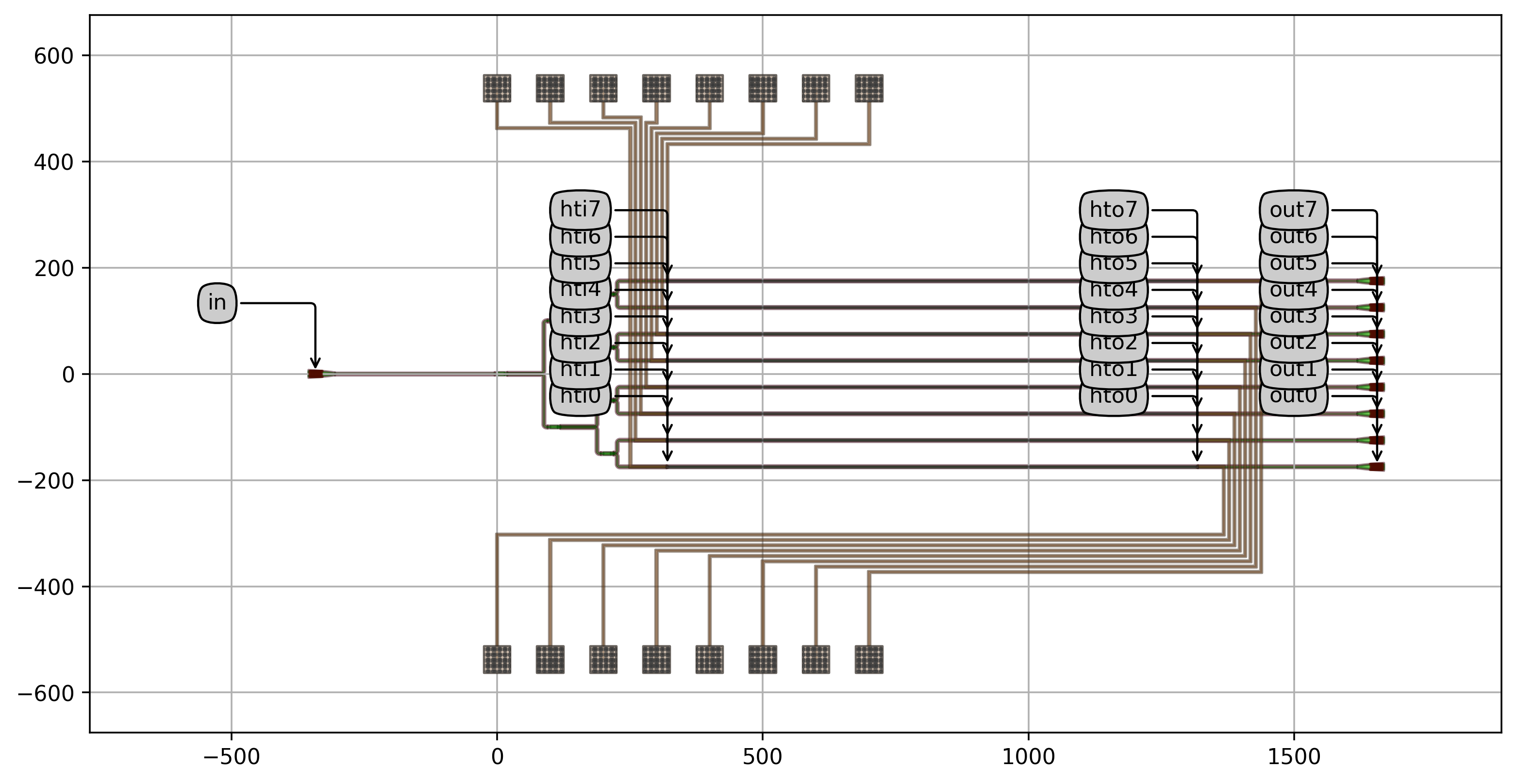
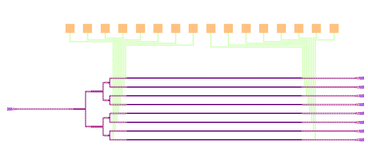
Extended example: Electrical routing to two sides
Instead of routing all the electrical connections of the OPA to one side (north), we can also define a PCell which routes them to two sides (north and south).
To obtain your OPA routed to two sides, you can use the PCell TwoSidesRoutedOPA, which is also defined in opa/cell.py.
Here below you may find the layout and the simulation of the OPA routed to two sides obtained by running the script example_twosides_routed_opa.py.