Designing a splitter tree
In this section, we are going to design a simple circuit layout: a splitter tree with two levels, made of three connected splitters with grating couplers at each input and output. The result is the following circuit with one input and four outputs.
Two-level splitter tree design
To do this we will use components that are already defined for us in a Process Design Kit (PDK). We will use the SiFab PDK which is included with your IPKISS installation and ready to use out of the box. It is a PDK built for training and demonstration purposes only.
If you want to find out more about using Design Kits, have a look at Installing Design Kits.
Building a circuit with i3.Circuit
A simple way to build a circuit in IPKISS is to use i3.Circuit, which allows you to easily define connectivity between a number of instances.
When placing these instances, i3.Circuit will generate all the waveguides needed to connect them together.
In the file 1_tutorials/1_splitter_tree.py, we are going to create the most basic circuit possible using i3.Circuit.
We will then build on this example to add functionality in the later files.
Let’s start with the circuit definition.
To define a circuit, we define a Python class that inherits from i3.Circuit in 1_splitter_tree.py and call it SplitterTree.
class SplitterTree(i3.Circuit):
To finish this class, we need the following ingredients:
Insts. This is a Python list containing
i3.Instspecs that define the instances in our circuit. We first need to import the MMI class we will use from thesi_fabPDK. In this case, we have three instances, one for each splitter. Therefore, we add three instances of this MMI.
luceda-academy/training/getting_started/2_circuit_layout/1_tutorials/1_splitter_tree.pydef _default_specs(self): # 1. We define the instances that form our circuit, via the i3.Inst spec. We have 3 splitters, 1 for the first # level and 2 for the second level. We call the MMI class from the si_fab PDK and pass this as the reference # argument, then add the three unique names for our instances as the first argument. mmi = pdk.MMI1x2Optimized1550() # importing an MMI from the si_fab PDK specs = [i3.Inst(["mmi_0", "mmi_1", "mmi_2"], mmi)]
Specs. This is a list containing all the layout specifications that apply to each component. Specifications can control the position of each instance, as well as the routing between them. Waveguide routing is defined between two optical ports, using a connector class, such as
ConnectBend. The ports are identified by the name of the instance and the name of the port using the formatinstance:port.luceda-academy/training/getting_started/2_circuit_layout/1_tutorials/1_splitter_tree.py# 2. We place the MMIs using coordinates relative to the origin, by adding placements into the specs list. # Then we can connect them using the connect methods in the same ways. To connect the bends, we use the optical # port names of the start and end of the waveguide. Port names are assigned in the MMI component and can be seen # by inspecting the MMI code in "pdks/si_fab/ipkiss/si_fab/components/mmi/pcell/cell.py". You can open this file # directly by holding "ctrl" and clicking on the "MMI1x2Optimized1550()" object in the _default_specs function. specs += [ i3.Place("mmi_0", (0, 0)), # Placing "mmi_0" at position (0,0) using "i3.Place()" i3.Place("mmi_1", (100, -25)), # try moving the MMIs by changing the coordinates and seeing what happens i3.Place("mmi_2", (100, 25)), ] # 3. We use the "i3.ConnectBend()" method to create waveguides between the MMIs in level one and two. We can # pass in a list of port name pairs to connect multiple ports at once. These names are defined by the # instance name, as well as the port names in the PDK component. specs += [ i3.ConnectBend([("mmi_0:out1", "mmi_1:in1"), ("mmi_0:out2", "mmi_2:in1")]), ] return specs
Now, we can instantiate the SplitterTree PCell in 1_splitter_tree.py and use .Layout() and .visualize() to view it.
    splitter_tree = SplitterTree()  # instantiate the SplitterTree class
    splitter_tree_layout = splitter_tree.Layout()  # call the Layout() method of the SplitterTree class
    splitter_tree_layout.visualize()  # call visualize to display the layout
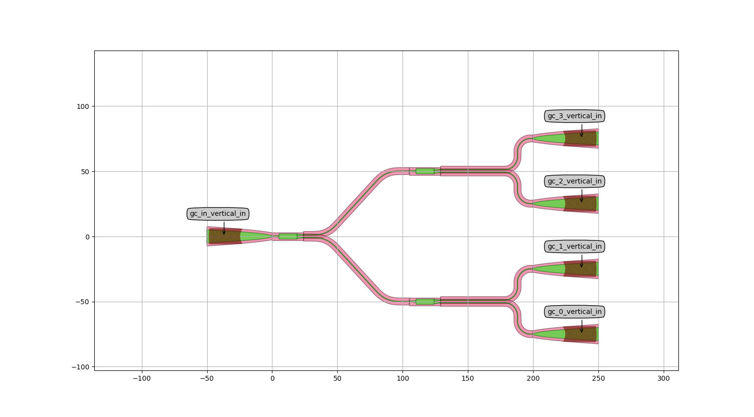
Splitter tree built with i3.Circuit
Placement
In the file 2_placement.py we are going to expand the previous circuit with some more advanced placement options, as well as adding grating couplers. We use the grating coupler class from our PDK to add instances to our specs, in the same way that we used the MMI class. For the output side, we are going to add four grating couplers using a combination of a python for loop and formatted string literal (commonly referred to as f-strings). This allows us to add them all in one loop.
    def _default_specs(self):
        mmi = pdk.MMI1x2Optimized1550()  # importing an MMI from the si_fab PDK
        gc = pdk.FC_TE_1550()  # importing a grating coupler from the si_fab PDK

        # 1. We have added a grating coupler from the si_fab PDK.
        # If you run this file, IPKISS Canvas will open and you can click on 'si_fab' in the left hand
        # pane to access all the components within the PDK.

        specs = [
            i3.Inst(["mmi_0", "mmi_1", "mmi_2"], mmi),
            i3.Inst("gc_in", gc),  # adding a grating coupler instance
        ]

        # 2. We can use a for loop to create names for multiple instances without typing them all out.
        # Below we use "f-strings" to add unique numbered names into a list.
        # The f"...{}" will read the content of the {} as a string, so we can pass in
        # the iterator (grating_number in this case) to the f-string to number all the instances.
        # To add to an instance we use a single i3.Inst with a list of names and a single reference.

        gc_names = []
        for grating_number in range(4):
            gc_names.append(f"gc_{grating_number}")

        specs.append(i3.Inst(gc_names, gc))
In the specs method we use a slightly different approach to add specifications than in the first script.
We first create an empty list called specs, then use the append method to add our specifications one at a time.
Using i3.Join and i3.Place gives additional freedom to your design, and helps when creating parametric layouts.
In Placement and Routing Reference you can find a full list of available specifications.
        specs = [
            i3.Inst(["mmi_0", "mmi_1", "mmi_2"], mmi),
            i3.Inst("gc_in", gc),  # adding a grating coupler instance
        ]

        # 2. We can use a for loop to create names for multiple instances without typing them all out.
        # Below we use "f-strings" to add unique numbered names into a list.
        # The f"...{}" will read the content of the {} as a string, so we can pass in
        # the iterator (grating_number in this case) to the f-string to number all the instances.
        # To add to an instance we use a single i3.Inst with a list of names and a single reference.

        gc_names = []
        for grating_number in range(4):
            gc_names.append(f"gc_{grating_number}")

        specs.append(i3.Inst(gc_names, gc))

        # 3. Create an empty list called specs that we can add to in the future. To add to it, we use "specs.append()"
        # which will add the contents of the brackets to the end of the specs list.

        specs.append(i3.Place("mmi_0:in1", (0, 0)))  # we can use the port names to place using the port coordinate

        # 4. We place the 1st MMI with respect to the 0th MMI using the i3.Place method with relative_to argument

        specs.append(i3.Place("mmi_1:in1", (100, -50), relative_to="mmi_0:out1"))
        specs.append(i3.Place("mmi_2:in1", (100, 50), relative_to="mmi_0:out2"))

        # 5. The i3.Join() method will directly connect two ports using their directions.

        specs.append(i3.Join("gc_in:out", "mmi_0:in1"))
        specs.append(i3.ConnectBend([["mmi_0:out1", "mmi_1:in1"], ["mmi_0:out2", "mmi_2:in1"]]))
It is also possible to use a for loop to add specifications in a programmatic way. Appending into a list allows us to use Python logic to add multiple specs instead of typing each one out one by one.
        for grating_number in range(4):
            specs.append(i3.Place(f"gc_{grating_number}:out", (200, -75 + grating_number * 50), angle=180))
Connectors
So far we have used the default ConnectBend class to generate all our waveguides.
Here we will see how to add arguments to this class to customize the waveguides, or use a new class ConnectManhattan.
If multiple connectors share the same properties (such as bend_radius and rounding_algorithm), then we can pass a list of the ports to create them together.
        # 1. We can add arguments to the ConnectBend() method to define certain properties of the connection, such
        # as the bend radius, or if we want a straight section before the bends. There are three included rounding
        # algorithms in IPKISS: ShapeRound, SplineRoundingAlgorithm and EulerRoundingAlgorithm. You can also
        # implement your own algorithm if you prefer.

        specs += [
            i3.ConnectBend(
                [("mmi_0:out1", "mmi_1:in1"), ("mmi_0:out2", "mmi_2:in1")],
                bend_radius=20,  # sets the bend radius
                start_straight=5,  # sets the length of the straight section at the start of the waveguide
                end_straight=5,  # sets the length of the straight section at the end of the waveguide
                rounding_algorithm=i3.EulerRoundingAlgorithm(),  # sets the rounding algorithm
            ),
        ]
Besides the ConnectBend class, there is another connector that is included as standard within IPKISS.
The ConnectManhattan class will route between two ports using only right-angled bends along the path.
It also supports the use of control points, which act as anchors that the waveguide must pass through.
Control points are great for custom routing and obstacle avoidance.
        # uses 90 degree bends. As with "i3.ConnectBend()" the bending algorithm can also be set, as well as other
        # parameters.

        specs += [
            i3.ConnectManhattan(
                [
                    ("mmi_1:out1", "gc_0:out"),
                    ("mmi_1:out2", "gc_1:out"),
                    ("mmi_2:out1", "gc_2:out"),
                    ("mmi_2:out2", "gc_3:out"),
                ],
                bend_radius=10,  # see what happens if you set the bend radius to be to too large (e.g. 15 and 20)
            )
        ]
Parameters
So far, all the circuits we have seen use hard-coded values for different parameters. This is great for keeping the examples easy to follow, however, to get the most value out of using IPKISS, we need to use parametric design principles. For example, we can create a parameter that corresponds to the vertical spacing between the output grating couplers (a common use case is the pitch of a fiber array) and use this to place all the gratings relative to each other.
To do this, we need to set up some properties in the class which correspond to all the variables we want to be able to change. These properties can be set when the class is instantiated to configure the class.
In many cases, it is useful to assign default values to these properties. That way, when you instantiate an object and do not specify a property value, the default value of that property will be used. This can be achieved in 2 ways:
Directly from the property definition line, using the argument
default=<something>.Through a default method, called
_default_<name_of_the_property>. The function returns the default value.
We can now write a general class that can be used in multiple different ways depending on the values we pass to the properties.
There are different restrictions we can place on these properties, which restrict the type of objects they can handle.
ChildCellProperty is used for the classes we are importing and the two PositiveNumberProperty are used to adjust the distance between the splitters and gratings in the circuit.
The ChildCellProperty is restricted so that it can only take an instance of a PCell, whilst the PositiveNumberProperty must take a positive number.
    gc = i3.ChildCellProperty(doc="Grating coupler used.")
    spacing_x = i3.PositiveNumberProperty(default=100.0, doc="Horizontal spacing between the splitter levels.")
    spacing_y = i3.PositiveNumberProperty(default=50.0, doc="Vertical spacing between the splitters in each level.")
The final ingredient we need to complete the layout of our circuit is to expose some ports in the circuit. We expose the ports using a dictionary where we can also rename the port names for our convenience.
    def _default_exposed_ports(self):
        exposed_ports = {
            "gc_in:vertical_in": "in",  # the "gc_in:vertical_in" port is renamed to "in"
            "gc_out_0:vertical_in": "out0",  # this renaming can shorten the names significantly and improve readability
            "gc_out_1:vertical_in": "out1",
            "gc_out_2:vertical_in": "out2",
            "gc_out_3:vertical_in": "out3",
        }
        return exposed_ports
Verification
With all the properties set up correctly, we can now call our class with different values for these properties and see how the circuit changes. There are multiple ways to visualize and verify the results, most notably:
visualize()to display the layout directly, using the Luceda Layout Visualizer.write_gdsii()to generate a GDS file, which can be opened by a third-party GDS viewer.to_canvas()to generate a schematic from the layout and display it in IPKISS Canvas.
Because IPKISS Canvas displays all available library components and their (port) names,
it is also a great tool to help you write code for the insts and specs of i3.Circuit.
    default_splitter_tree = SplitterTree(spacing_x=50, spacing_y=100)  # change the spacing_x and spacing_y parameters
    default_splitter_tree_layout = default_splitter_tree.Layout()
    # Right-click in Canvas and select "Rearrange Circuit".
    default_splitter_tree_layout.to_canvas(project_name="splitter_tree")
    default_splitter_tree_layout.write_gdsii("splitter_tree.gds")
    default_splitter_tree_layout.visualize()
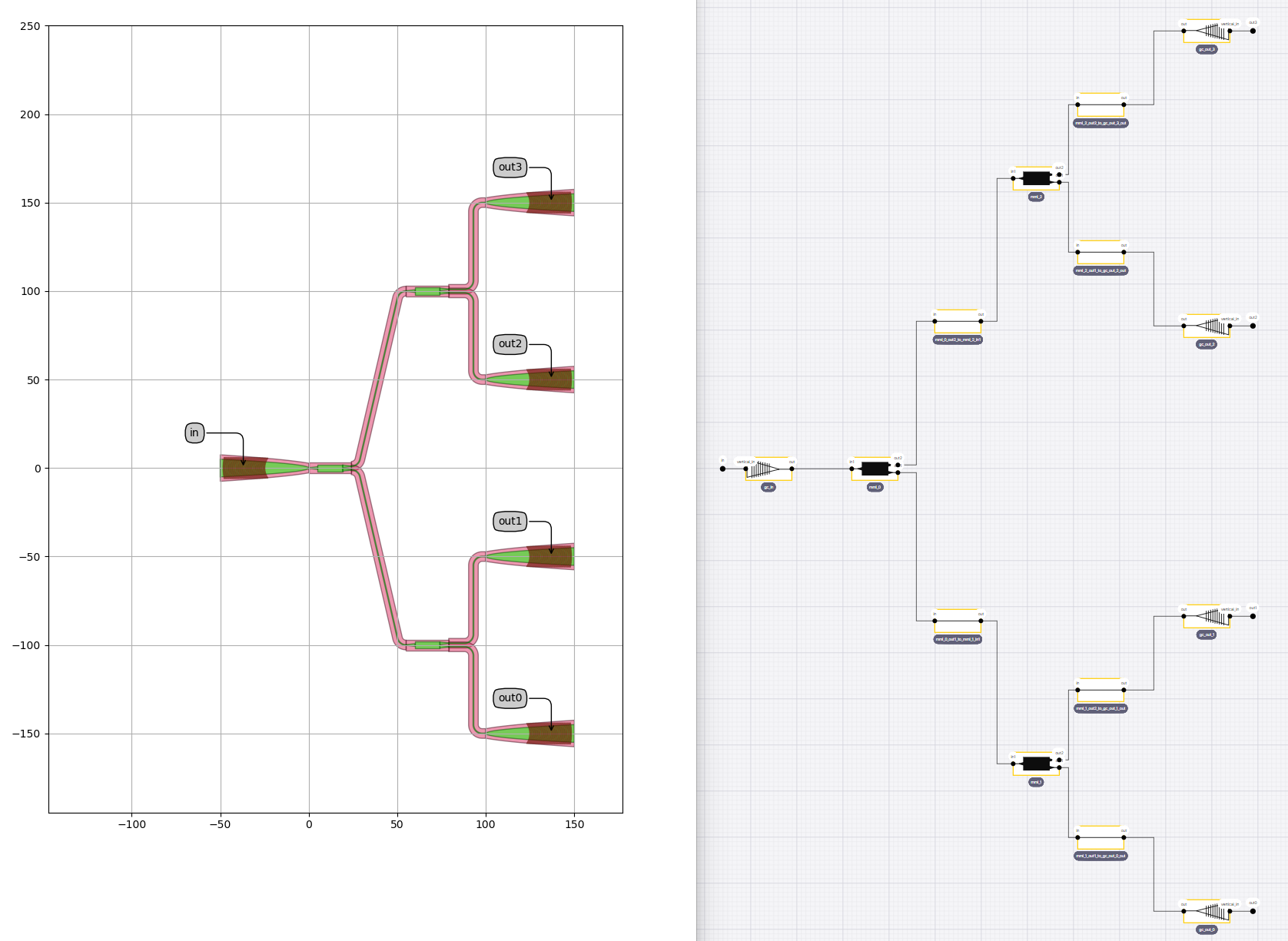
Our splitter tree design, visualized using Matplotlib on the left and IPKISS Canvas on the right.
When we call the class in our code we can change the distances between the splitters, or even what class we use to create the splitters, by changing the parameters we pass into the class.
    splitter_tree = SplitterTree(splitter=splitter, spacing_x=30, spacing_y=30)
    splitter_tree_layout = splitter_tree.Layout()
    splitter_tree_layout.write_gdsii("splitter_tree_2.gds")
    splitter_tree_layout.visualize()
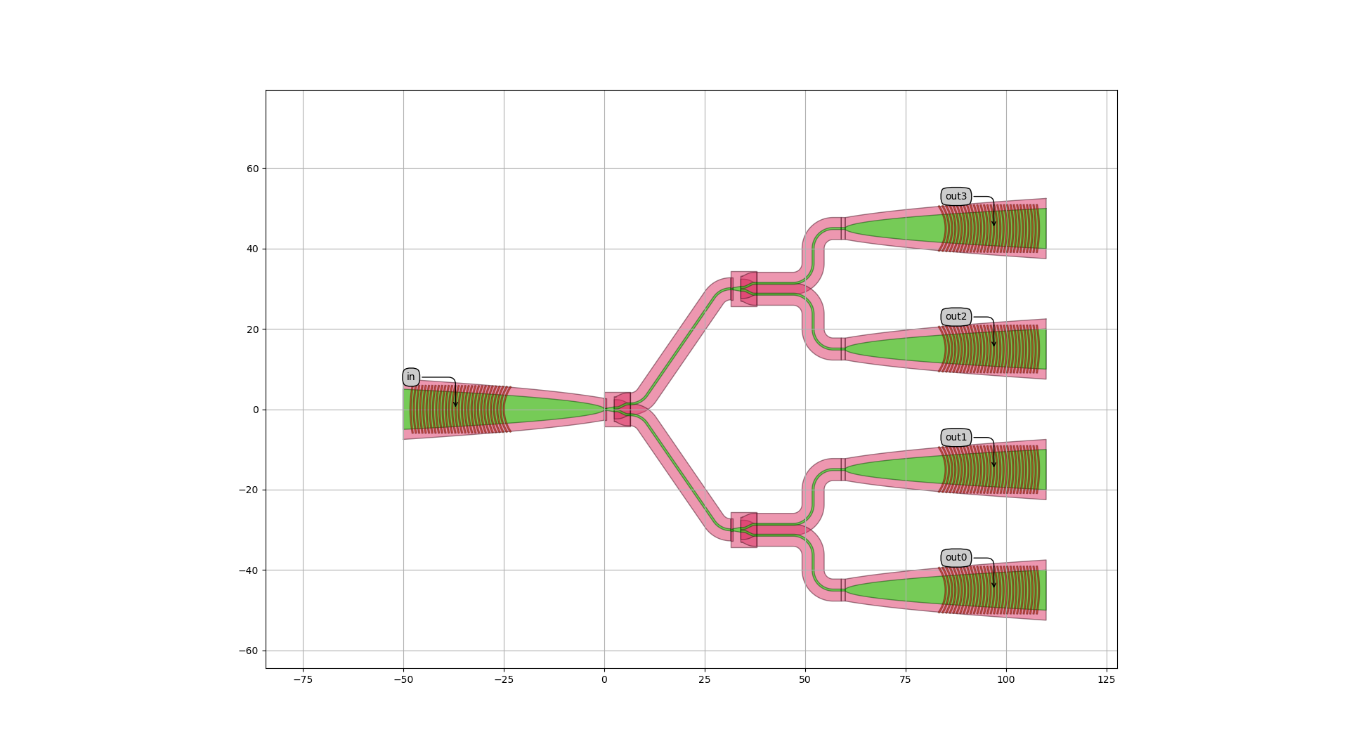
Splitter tree with customized splitter and spacing
Exercise
Now that we have learned how to create the layout of a circuit, let’s apply what we learned to extend this example to a three-level splitter tree. In the path getting_started/2_circuit_layout/2_exercises/exercises.py, you will find an incomplete circuit. There are ellipses in various locations which show you where some code needs to be added. Try to complete it, and use the solutions supplied if you get stuck.