ConnectBend
- class ipkiss3.all.ConnectBend
Connector for creating an as simple as possible bend between two optical ports based on the given rounding parameters.
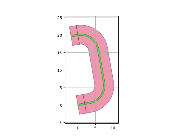
When possible, a single arc bend is used. When the ports are (almost) pointing towards each other, this yields an (pseudo) S-bend. When the ports are (almost) aligned, this yields a (pseudo) U-bend.
ConnectBend tries to handle as much cases as possible, but it does not guarantee that the routes are optimal or that there are no crossings. If no valid route could be calculated with the given rounding algorithm and parameters, an exception is raised.
This connector is supposed to be used together with
i3.place_and_route.- Parameters:
- min_spacing: float and int, float, integer, floating and number >= 0, optional
minimal spacing between parallel sections of the route
- angle_step: float, optional
Angle step to be used in the bends
- end_straight: float and int, float, integer, floating and number >= 0, optional
Straight length before the end port.
- start_straight: float and int, float, integer, floating and number >= 0, optional
Straight length after the start port.
- bend_radius: float and number > 0, optional
Bend radius.
- rounding_algorithm: optional
Rounding algorithm (ShapeRound, ShapeRoundAdiabaticSpline, …). Takes a shape as input and returns a new (rounded) shape.
- end_taper_length: ( float and int, float, integer, floating and number >= 0 ), optional, *None allowed*
Length of the taper for the transition to be generated at the end of the connection if the trace templates mismatch. If it is not specified, a default transition from the database will be used.
- start_taper_length: ( float and int, float, integer, floating and number >= 0 ), optional, *None allowed*
Length of the taper for the transition to be generated at the start of the connection if the trace templates mismatch. If it is not specified, a default transition from the database will be used.
- trace_template: ( PCell and _TraceTemplate ), optional, *None allowed*
Trace template to use for the waveguide between the two ports, when the ports have a different template, transitions will be added. When this property is left unspecified/None the trace_template of the start_port will be used
See also
Examples
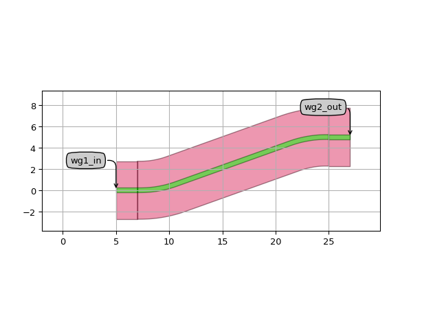
import ipkiss3.all as i3

# Define waveguide
wg = i3.Waveguide()

# Create circuit
circuit = i3.Circuit(
    specs=[
        i3.Inst(["wg1", "wg2"], wg),
        i3.Place("wg1", (5, 0)),
        i3.Place("wg2", (25, 5)),
        i3.ConnectBend("wg1:out", "wg2:in", bend_radius=10),
    ],
)
circuit_layout = circuit.Layout()
circuit_layout.visualize(annotate=True)
import ipkiss3.all as i3

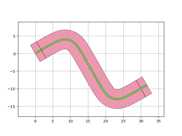
ra = i3.SplineRoundingAlgorithm(adiabatic_angles=(20.0, 20.0))

# Define waveguide
wg = i3.Waveguide()

# Create circuit
circuit = i3.Circuit(
    specs=[
        i3.Inst(["wg1", "wg2"], wg),
        i3.Place("wg1", (0, 0), angle=30),
        i3.Place("wg2", (30, -10), angle=30),
        i3.ConnectBend("wg1:out", "wg2:in", rounding_algorithm=ra, bend_radius=4),
    ],
)
circuit_layout = circuit.Layout()
circuit_layout.visualize()
import ipkiss3.all as i3

# Define waveguide
wg = i3.Waveguide()

# Create circuit
circuit = i3.Circuit(
    specs=[
        i3.Inst(["wg1", "wg2"], wg),
        i3.Place("wg1", (0, 0), angle=10),
        i3.Place("wg2", (0, 20), angle=190),
        i3.ConnectBend("wg1:out", "wg2:in"),
    ],
)
circuit_layout = circuit.Layout()
circuit_layout.visualize()
import ipkiss3.all as i3

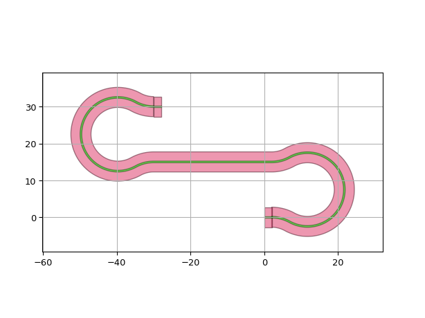
# Define waveguide
wg = i3.Waveguide()
bend_radius = 10

# Create circuits
ra = i3.ShapeRound
circuit = i3.Circuit(
    specs=[
        i3.Inst("wg1", wg),
        i3.Inst("wg2", wg),
        i3.Place("wg1", (0, 0)),
        i3.Place("wg2", (-30, 30)),
        i3.ConnectBend("wg1:out", "wg2:in", bend_radius=bend_radius, rounding_algorithm=ra),
    ],
)
circuit_layout = circuit.Layout()
circuit_layout.visualize()

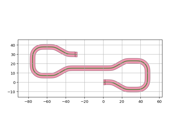
ra = i3.SplineRoundingAlgorithm(adiabatic_angles=(10, 10))
circuit = i3.Circuit(
    specs=[
        i3.Inst(["wg1", "wg2"], wg),
        i3.Place("wg1", (0, 0)),
        i3.Place("wg2", (-30, 30)),
        i3.ConnectBend("wg1:out", "wg2:in", bend_radius=bend_radius, rounding_algorithm=ra),
    ],
)
circuit_layout = circuit.Layout()
circuit_layout.visualize()
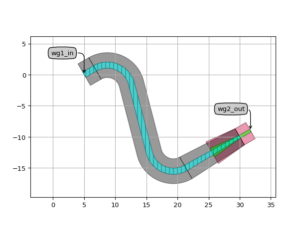
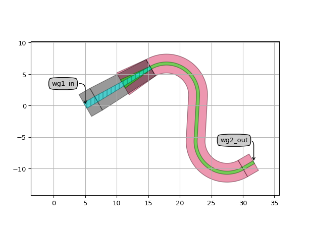
ConnectBend will automatically introduce tapers when required to connect the ports together.:
import si_fab.all as pdk  # noqa
from picazzo3.traces.wire_wg.trace import WireWaveguideTemplate
from picazzo3.traces.rib_wg.trace import RibWaveguideTemplate
import ipkiss3.all as i3

rib_tpl = RibWaveguideTemplate()
rib_tpl.Layout(
    core_width=1.0,
    cladding_width=4.0,
)

wire_tpl = WireWaveguideTemplate()
wire_tpl.Layout(core_width=0.5, cladding_width=3)

# connect the ports
circuit = i3.Circuit(
    specs=[
        i3.Inst("wg1", i3.Waveguide(trace_template=rib_tpl)),
        i3.Inst("wg2", i3.Waveguide(trace_template=wire_tpl)),
        i3.Place("wg1", (5, 0), angle=30),
        i3.Place("wg2", (30, -10), angle=30),
        i3.ConnectBend("wg1:out", "wg2:in", bend_radius=4),
    ],
)
circuit_layout = circuit.Layout()
circuit_layout.visualize(annotate=True)

# you can also set the desired trace_template for the
# connection:
circuit = i3.Circuit(
    specs=[
        i3.Inst("wg1", i3.Waveguide(trace_template=rib_tpl)),
        i3.Inst("wg2", i3.Waveguide(trace_template=wire_tpl)),
        i3.Place("wg1", (5, 0), angle=30),
        i3.Place("wg2", (30, -10), angle=30),
        i3.ConnectBend("wg1:out", "wg2:in", trace_template=wire_tpl),
    ],
)
circuit_layout = circuit.Layout()
circuit_layout.visualize(annotate=True)
