OpenLight: 400G Optical Transceiver
A 400G transceiver is a high-speed optical transceiver capable of transmitting and receiving data at a rate of 400 gigabits per second (Gbps). These transceivers are typically used in data center networks, telecommunications infrastructure, and high-performance computing environments where extremely fast data transmission is required. They play a crucial role in enabling the high-speed connectivity necessary for handling large volumes of data in modern network infrastructures.
The Luceda Photonics Design Platform is ideal for designing and verifying Photonic Integrated Circuits (PICs) as it offers parametric control over the layout. The platform also provides various tools for layout verification, using both a scripting approach and schematic capture. In this tutorial, we will showcase the design of the transmitter part of a 400G transceiver PIC using the OpenLight PDK.
Note
To run the example in the software and see the design GDSII file, you need access to the OpenLight PDK. Please contact Tower Semiconductor and sign an NDA to obtain the PDK.
The methodology used here can be easily applied to the receiver part of the transceiver.
We first draw a schematic of a single-channel transmitter in IPKISS Canvas. It allows us to easily communicate around the design process within the team. More details about schematic design in IPKISS Canvas environment can be found in Introduction to IPKISS Canvas for schematic capture.
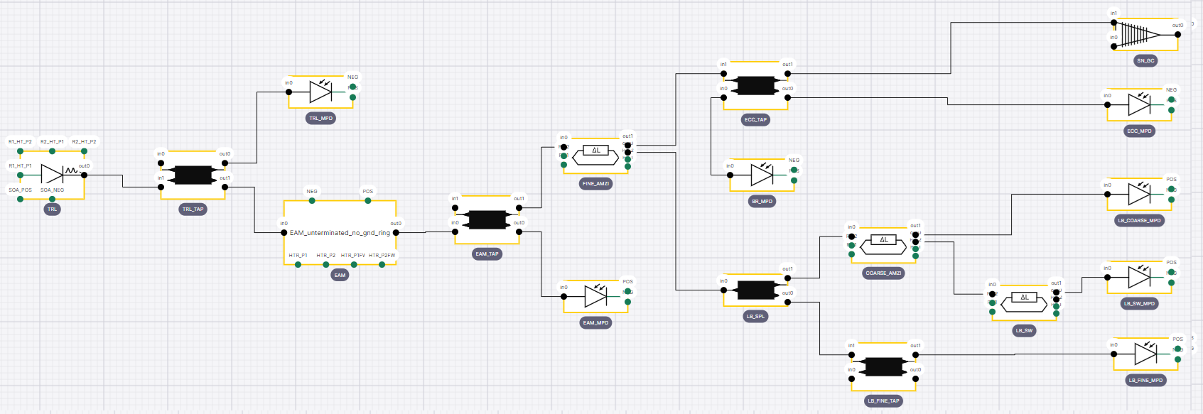
Figure 1. Optical schematic of a single-channel transmitter PIC.
Introduction
The building blocks of the transmitter circuit are based on OpenLight PDK components including grating couplers, symmetric and asymmetric Mach-Zehnder interferometer (MZI) switches, electro-absorption modulators (EAM), monitor phase detectors (MPD), tunable ring lasers (TRL), bond pads, and multi mode interferometers (MMIs).
In this application example, we will go through the following steps:
First, since there are several components that are connected to nearby bondpads, we create PCells that consist of these components and the bondpads they are connected to. We do this for symmetric and asymmetric MZIs, MPDs, and laser. This way, we avoid complexity and potential errors that might raise by doing this at the top level.
Second, we create a library on top of the PDK to maintain these cells in a structured way. It reduces the complexity of any individual file, and makes it easy to find and fix mistakes. More information about the library organization can be found in Building a user library.
Third, we design the 1-channel transmitter PIC.
Fourth, we use the single-channel transmitter to build a four-channel transmitter.
Finally, we use a range of verification tools in both the code and Canvas environments to ensure the validity of our design.
Organizing the library
To simplify a complex design, we can break it into different levels of hierarchy. Each level can be imported into a higher level of hierarchy without making one design too complex. It will also help other people in the team to understand the design better and allows for these smaller building blocks to be reused in other work, adding to their value. In addition, it makes debugging in case of errors or fine grained testing of your components easier (Luceda IP Manager). The library components can be used within other library components. For example, in the optical transmitter design, a pair of bond pads that are electrically connected have been added to other components in the library. One of the foundry’s design rules requires a minimum spacing of 150 µm between the center of the bond pads. We set this as a parameter in the BondPadPair class, which is used to instantiate pairs of bond pads. Additionally, we can set the trace template of the electrical connection between these bond pads as a parameter. The code below demonstrates the parameterized BondPadPair class.
from openlight_ph18da import all as pdk

from ipkiss3 import all as i3


class BondPadPair(i3.Circuit):
    """A pair of bondpads on the METAL2 layer that are electrically connected together"""

    bondpad_spacing = i3.PositiveNumberProperty(default=150, doc="Spacing between bondpads.")
    electrical_tt = i3.TraceTemplateProperty(doc="Trace template of the metal routing.")

    def _default_electrical_tt(self):
        ett = pdk.Metal2WireTemplate()
        ett_lo = ett.Layout(width=80.0)
        return ett_lo

    def _default_specs(self):
        bondpad_m2 = pdk.bondpad_m1m2()
        return [
            i3.Inst(["bp1", "bp2"], bondpad_m2),
            i3.Place("bp1", (0, 0)),
            i3.Place("bp2", (self.bondpad_spacing, 0), relative_to="bp1"),
            i3.ConnectElectrical("bp1:P1", "bp2:P1", end_angle=180, trace_template=self.electrical_tt),
        ]
Once the library components are designed, they can be imported in the design file just like importing the PDK:
from openlight_ph18da import all as pdk
from ipkiss3 import all as i3
from pteam_library_openlight import all as lib
Single-channel transmitter
Many circuits, including the single-channel transmitter we have designed in luceda-academy/training/topical_training/optical_transceiver/transmitter/cell/single_ch_cell.py, contain components that the designer may want to change to suit a design need. In this case, we have chosen to define all the components as a property of the class. This allows for maximum flexibility, as the designer may later decide to use a different splitter or grating coupler, defining a new class for the transmitter. Additionally, to reduce design errors, we set some constants to use, for example for the bend radii and spacing between the cells in horizontal and vertical directions.
The following code snippet shows how we can define parameters as the class properties:
    bend_radius = i3.PositiveNumberProperty(default=40, doc="Minimum bend radius.")
    # Define some spacing values as parameter to avoid hard coding the spacings as much as possible
    spacing_a = i3.PositiveNumberProperty(default=400, doc="First spacing value between instances.")
    spacing_b = i3.PositiveNumberProperty(default=100, doc="Second spacing value between instances.")

    trl = i3.ChildCellProperty(doc="laser")
    tap = i3.ChildCellProperty(doc="tap")
    mpd = i3.ChildCellProperty(doc="mpd")
    eam = i3.ChildCellProperty(doc="electroapsorption modulator")
    amzi = i3.ChildCellProperty(doc="asymmetric MZI switch")
    spl = i3.ChildCellProperty(doc="splitter")
    fine_mpd = i3.ChildCellProperty(doc="fine mpd")
    sw = i3.ChildCellProperty(doc="switch")
    gc = i3.ChildCellProperty(doc="grating coupler")
    terminator = i3.ChildCellProperty(doc="terminator")

    def _default_trl(self):
        return lib.TRLWithPads()

    def _default_mpd(self):
        return lib.MPDWithPads()

    def _default_amzi(self):
        return lib.AMZISwitchOnePortWithPads()

    def _default_fine_mpd(self):
        return lib.FineMPDWithPads()

    def _default_sw(self):
        return lib.SMZISwitchOnePortWithPads()

    def _default_tap(self):
        return pdk.bmmi()

    def _default_eam(self):
        return pdk.EAM_unterminated_no_gnd_ring()

    def _default_spl(self):
        return pdk.mmi_1x2()

    def _default_gc(self):
        return pdk.gc_oip()

    def _default_terminator(self):
        return pdk.SiTerminator()
After importing all the building blocks and setting the circuit properties, we can proceed to define the instances and specifications. Components that are used only once or twice can be individually specified within the instances dictionary. For components that are used more frequently, we can efficiently define the instances using for loops:
    def _default_specs(self):
        specs = [
            i3.Inst("TRL", self.trl),
            i3.Inst("EAM", self.eam),
            i3.Inst("FINE_AMZI", self.amzi),
            i3.Inst("LB_SPL", self.spl),
            i3.Inst("COARSE_AMZI", self.amzi),
            i3.Inst("LB_SW", self.sw),
            i3.Inst("SN_GC", self.gc),
        ]
        # 4 taps (bmmi) are used in a single-channel transmitter circuit
        specs.append(
            i3.Inst(["TRL_TAP", "EAM_TAP", "LB_FINE_TAP", "ECC_TAP"], self.tap),
        )

        # 4 mpds are used in a single-channel transmitter circuit
        specs.append(
            i3.Inst(["TRL_MPD", "EAM_MPD", "BR_MPD", "ECC_MPD"], self.mpd),
        )

        # 3 fine mpds are used in a single-channel transmitter circuit
        specs.append(
            i3.Inst(["LB_FINE_MPD", "LB_COARSE_MPD", "LB_SW_MPD"], self.fine_mpd),
        )

        # Instantiate 3 terminators that should be joined to the unconnected ports in the single-channel transmitter PIC
        specs.append(
            i3.Inst([f"terminator_{terminator_number}" for terminator_number in range(3)], self.terminator),
        )
The specification list contains various statements for placement and routing.
For placement, you can use commands such as i3.Place, i3.FlipV, i3.FlipH, among others.
For routing, the connectors i3.ConnectBend and i3.ConnectManhattan and more are available.
Additionally, control points can be added to customize the path of a connection.
The following code snippet within the specifications list for the single-channel transmitter class demonstrates how to use a control point within the i3.ConnectManhattan connector.
This example specifies that the waveguide connecting the ports “LB_COARSE_MPD:in0” and “COARSE_AMZI:out1” should include a horizontal segment positioned -75 micrometers to the south of the “LB_SW” component.
The distance is measured from the bounding box encompassing the “LB_SW” component.
            # using control points to avoid obstacles
            i3.ConnectManhattan(
                "LB_COARSE_MPD:in0",
                "COARSE_AMZI:out1",
                control_points=[i3.H(-75, relative_to="LB_SW@S")],
                bend_radius=self.bend_radius,
            ),
It is also possible to use for loops to define the specifications. For example, four instances of the single-channel class are placed on top of each other using the following simple logic inside the specifications list of the four-channel transmitter class:
        # placing single-channel transmitter instances using for loop
        for transmitter_number in range(4):
            specs.append(
                i3.Place(
                    f"ch_{transmitter_number}",
                    (0, -transmitter_number * 1100),
                )
            )
To see how we implemented other specifications in this example, please refer to the _default_specs function in luceda-academy/training/topical_training/optical_transceiver/transmitter/cell/single_ch_cell.py and luceda-academy/training/topical_training/optical_transceiver/transmitter/cell/four_ch_cell.py.
Once the instances and specifications are defined in the single-channel transmitter class, we can instantiate its layout and visualize it.
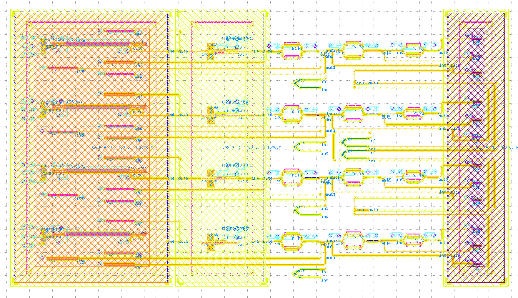
The following image shows the layout of the design:
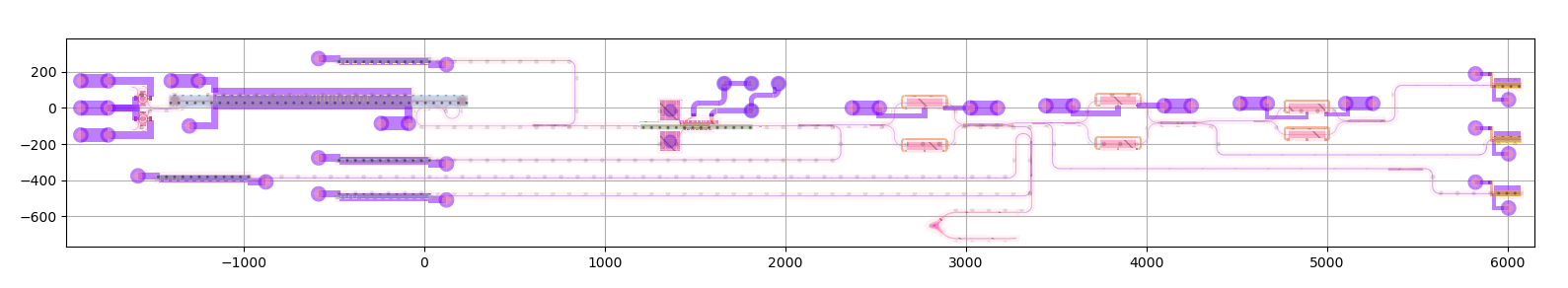
Figure 2. Visualization of the single-channel transmitter PIC in IPKISS.
Design verification in Canvas
Due to the complexity of the layout, it is difficult to verify the design by checking the GDSII file. To do this properly, we need to use more advanced tools. With IPKISS Canvas we can easily visualize the schematic and inspect different parameters of the circuit. The schematic we see in IPKISS Canvas is extracted directly from our layout, ensuring an exact match between the schematic representation and the real layout. Before exporting the whole design to Canvas, we can build a .iclib file for the library components and assign relevant symbols for them that describes its functionality. This helps designers in a team to quickly see the building blocks of the circuit. The following code can be used for this purpose and should be placed in the building folder of the library luceda_academy/libraries/pteam_library_openlight/building/build_iclib.py. It will generate the pteam_library_openlight.iclib file and would save it in luceda_academy/pteam_library_openlight/ipkiss. In addition, parameters of the symbol such as the position and domain of the ports can be adjusted from within Canvas.
import openlight_ph18da.all as pdk  # noqa
from ipkiss3.serdes.canvas.export_pdk import export_ipkiss_library
import os
import ipkiss3.all as i3

curdir = os.path.dirname(os.path.abspath(__file__))
ol_dir = os.path.abspath(os.path.join(curdir, 3 * (os.path.pardir + os.path.sep)))  # 5 directory levels up
ol_library_src_path = os.path.join(curdir, os.pardir, "ipkiss", "pteam_library_openlight")
library_name = "pteam_library_openlight"
export_ipkiss_library(
    library_name=library_name,
    library_path=ol_library_src_path,
    output_path=os.path.join(ol_library_src_path, f"{library_name}.iclib"),
    symbols={
        "TRLWithPads": {
            "image": i3.canvas.SymbolImage.Laser,
        },
        "AMZISwitchOnePortWithPads": {
            "image": i3.canvas.SymbolImage.MZI,
        },
        "SMZISwitchOnePortWithPads": {
            "image": i3.canvas.SymbolImage.MZI,
        },
        "BondPadPair": {
            "image": i3.canvas.SymbolImage.BondPad,
        },
    },
)
We can now export the design to Canvas by using to_canvas command after instantiating the layout of the single-channel transmitter.
transmitter = SingleTransmitter()
transmitter_lo = transmitter.Layout()
transmitter_lo.to_canvas(project_name="single_ch_transmitter", netlist_extraction_settings=settings)
Figure 3. shows the schematic capture of the circuit. Several checks can be done in the Canvas environment.
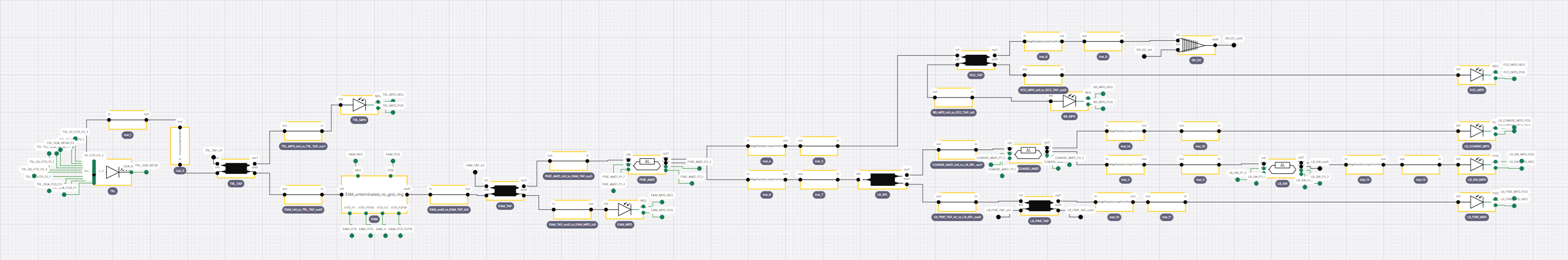
Figure 3. Schematic capture of single-channel transmitter in IPKISS Canvas.
The first step is to verify the interconnectivity between the building blocks. We can combine the initial schematic shown in Figure 1 and the Canvas schematic in Figure 3 to see whether the connected components match.
Figure 4. The exported layout in Canvas can be easily compared to the initial schematic design.
The only difference that can be seen is that in the exported schematic we also see the waveguides and transitions (generated when the trace templates of the connected ports are different) as blocks.
Let’s have a closer look at a part of the schematic of the circuit in Canvas:
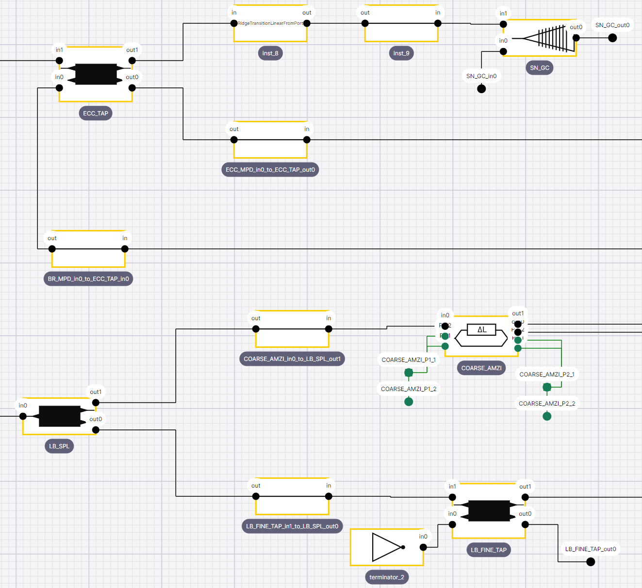
The unconnected ports and missing waveguides are easily observed. For example, the ‘LB_FINE_TAP_in0’ and the ‘LB_FINE_TAP_out0’ ports of the ‘LB_FINE_TAP’ are not connected to anything. The designer then can decide whether there are missing connections corresponding to them or leave them as they are.
We also see that the connection between “LB_SPL” and “COARSE_AMZI” is named “COARSE_AMZI_in0_to_LB_SPL_out1”. By clicking on it and pressing P key, a window with the component (a waveguide in this case) properties will pop up. From there, it is possible to inspect different properties of the connection such as the bend radius and the length of the connection:
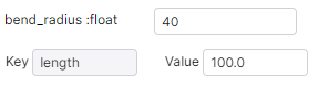
From here, we can see that the bend radius matches the value we set in the layout single-channel circuit parameters.
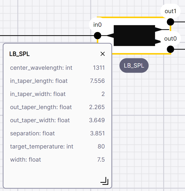
It is also possible to see the design specifications of the components. For example, different parameter values for LB_SPL MMI are presented by right-clicking on it and selecting ‘show card’:
Now we inspected the components, waveguides and their parameters using IPKISS Canvas, the next step is to design a 4-channel transmitter. This can be done by putting four instances of the designed single-channel together and adding a few more components that are shared between the channels. To achieve efficient photon emission or detection, certain components like lasers and monitor phase detectors should be placed under an epitaxial layer in the circuit. Therefore, we place appropriate epi cells from the PDK where these components are located.
        specs = [
            i3.Inst("PWR_COMB1and2", self.pwr_comb),
            i3.Inst("PWR_COMB3and4", self.pwr_comb),
            i3.Inst(["gc1and4", "gc2and3"], self.gc),
            i3.Inst("epi_gain", self.epi_gain),
            i3.Inst("epi_mpd_det", self.epi_mpd_det),
            i3.Inst("epi_eam", self.epi_eam),
        ]
Tape-out Preparation
Patching acute angles
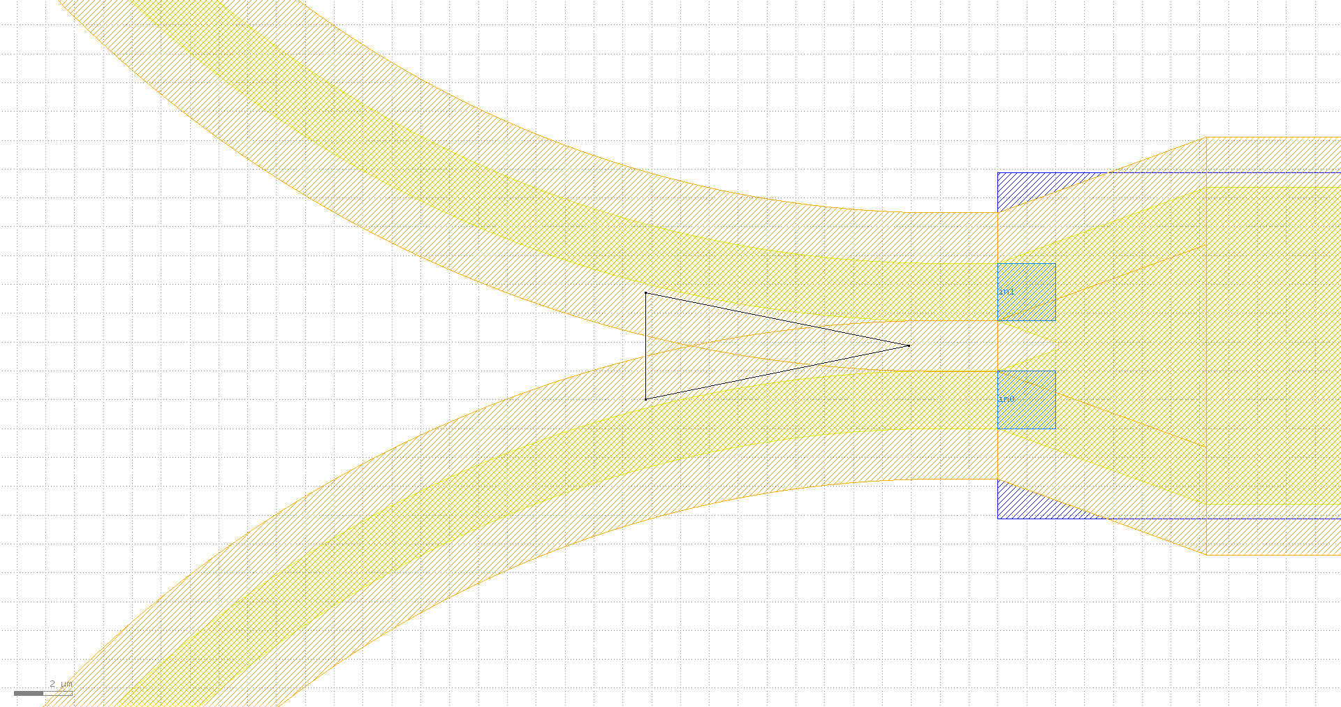
If we zoom into the design we see acute angles which violate the Design Rule Checks (DRC). The following image shows an acute angle between two rib waveguides that are connected to the MMI ports.
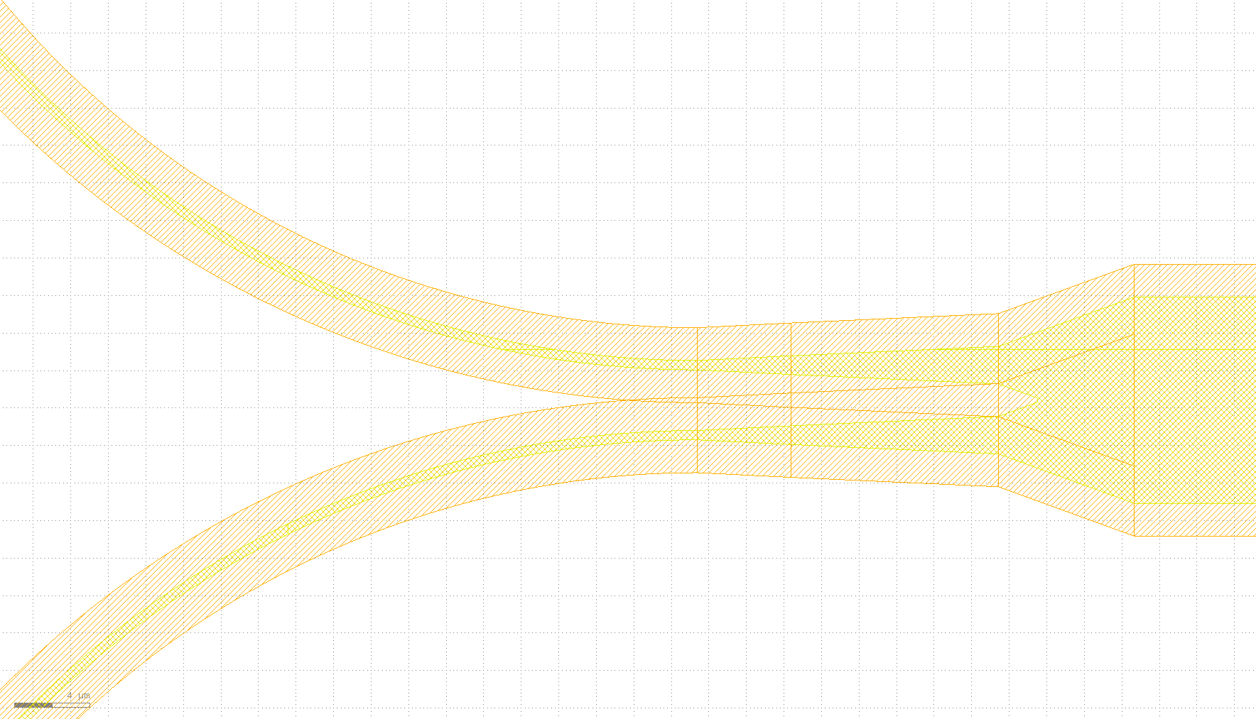
We can patch acute angles by detecting them in all layers (or a set of user chosen layers) and adding or subtracting stub elements to them.
transmitter = Transmitter()
transmitter_circuit_lo = transmitter.Layout()
elems_add, elems_subt = i3.get_stub_elements(transmitter_circuit_lo, stub_width=5, grow_amount=1)
stubbed_ch_lo = i3.LayoutCell().Layout(elements=elems_add + transmitter_circuit_lo.layout)
stubbed_ch_lo.write_gdsii("four_ch_stubbed.gds")
Bond pad spacing verification
It is important to keep the distance between bond pads greater than a specified minimum value to ensure manufacturability, proper electrical isolation and temperature management. This minimum distance is typically determined by the foundry. In this design using the OpenLight PDK, we have placed the bond pads of the single-channel transmitter to ensure a minimum center-to-center distance of 150 µm between them. We can write a Python function to calculate the distances between all combinations of points. These points can represent the positions of electrical or optical ports. Additionally, we can specify a minimum allowable distance, and the function will then identify and print any pairs of points that are too close, along with their corresponding distances. To identify all the electrical ports in our circuit, we can use .Layout().electrical_ports for the circuit class, as demonstrated in the code below. We then pass the list of electrical ports to the verify_min_distance function, along with the specified minimum distance. This approach can be similarly applied to optical ports.
def verify_min_distance(ports, min_distance=10):
    def calculate_distance(port1, port2):
        x1, y1 = port1.position
        x2, y2 = port2.position
        distance = round(math.sqrt((x2 - x1) ** 2 + (y2 - y1) ** 2), 7)
        return distance

    ports_too_close = []
    for i in range(len(ports)):
        for j in range(i + 1, len(ports)):
            distance = calculate_distance(ports[i], ports[j])
            if distance < min_distance:
                ports_too_close.append((ports[i], ports[j], distance))

    if len(ports_too_close) > 0:
        print(f"Ports that are closer than the minimum distance {min_distance}:")
        for pa, pb, dist in ports_too_close:
            print(f"port {pa.name} is too close to port {pb.name}, distance = {dist}")
    else:
        print("Ports have enough distance between them.")

    return ports_too_close


if __name__ == "__main__":
    layout = Transmitter().Layout()
    ports = layout.electrical_ports
    verify_min_distance(ports, min_distance=150)
If we run the optical_transceiver/transmitter/port_spacing_calculation.py file, we will see that the statement ‘Ports have enough distance between them.’ will be printed.
Path-length matching
In some cases, it’s crucial to ensure that the lengths of certain connections are equal.
Using i3.path_length we can examine the lengths of our connections.
With i3.MatchLength we can do relative and absolute length matching.
For example, in the four-channel transmitter design, we may need the connections reference_a_wg1 and reference_a_wg2 shown in the following picture to be of equal length.
To achieve a good phase matching, we also need the number of bends in these connections to be equal.
This means extending the length of reference_a_wg2 so that it matches reference_a_wg1 in length and number of bends.
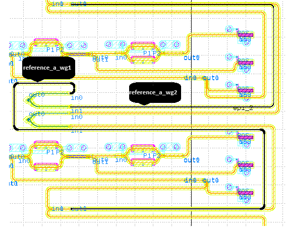
Now reference_a_wg_2 only has 2 bends, but if we add 4 control points to this connection both of the connections will have 6 bends. In order to achieve length matching we make sure that one of the vertical control points is flexible, so that IPKISS can move it around. Finally, this is how the length of reference_a_wg2 can be made to match the length of reference_a_wg1:
                # reference_a_wg2
                i3.ConnectManhattan(
                    "gc1and4:in1",
                    "PWR_COMB1and2:out0",
                    "reference_a_wg2",
                    control_points=[
                        i3.V(2550, relative_to="gc1and4:in1"),
                        i3.H(500, relative_to="gc1and4:in1"),
                        i3.V(2200, relative_to="gc1and4:in1", flexible=True),
                        i3.H(600 + 2 * self.bend_radius, relative_to="gc1and4:in1"),
                        i3.V(2550, relative_to="gc1and4:in1"),
                    ],
                    match_path_length=i3.MatchLength(reference="reference_a_wg1"),
                    min_straight=0,
                    bend_radius=self.bend_radius,
                ),
Running the example, you will see a warning about IPKISS being unable to determine the length of the transition.
For any component without the trace_length method implemented, zero length will be assumed.
If you need the exact length, e.g. for absolute length matching, you will need to register it manually, see the examples in i3.MatchLength.
In our case, we want the length of two connectors to be equal, hence this is not a problem as long as the connectors in question have the same number of transitions (and the transitions are identical).
Note
This example is intended to demonstrate the use of a PDK. While the design has undergone several checks, further modifications may be necessary to ensure it functions as a real, working circuit.
To run the example in the software and see the design GDSII file, you need access to the OpenLight PDK. Please contact Tower Semiconductor and sign an NDA to obtain the PDK. Once you have access, you can run the example in the software, located at: luceda-academy/training/topical_training/optical_transceiver/transmitter/cell/example_four_ch.py.
The exported schematics may need to be manually rearranged for better visualization.