SiEPIC Shuksan: Optical phased array (OPA)
Note
This tutorial requires the Luceda PDK for SiEPIC Shuksan, which is downloaded together with the Luceda Academy samples.
In this training, we focus on the design of an optical phased array (OPA) using the Luceda PDK for SiEPIC Shuksan. More specifically, we will show you how to create the layout of the first OPA described in the SiEPIC Shuksan design manual on page 24, called OPA1, and we will discuss how to simulate this device. Keeping in mind the principles introduced in the generic OPA training on Luceda Academy, we will first discuss the main building blocks associated with OPA1, before describing the layout and simulation of the actual OPA:
Laser
Splitter tree
Heated spirals matrix
Grating couplers matrix
Optical and electric routing
Laser source
The SiEPIC Shuksan PDK provides lasers as standard building blocks. There are 4 different laser versions having center wavelengths at 1270 nm, 1290 nm, 1310 nm and 1330 nm. These lasers have one optical and two electrical ports that are connected to the silicon chip through one photonic and two electric wirebonds. The designer does not need to draw those wirebonds; only the black box of the laser that the user wants to use needs to be drawn (see example of laser black box below). Later on, we will make sure neither the waveguides, nor the electrical wires will overlap with this black box, as required by the SiEPIC Shuksan design manual. In this example, we use the laser operating at 1270 nm, which is also the default wavelength of the OPA.
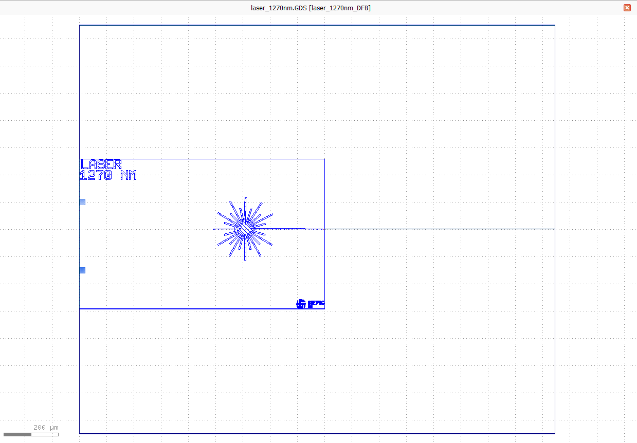
GDS file of the laser emitting light at 1270 nm center wavelength.
Splitter tree
The splitter tree is very similar to the splitter tree discussed in a related OPA tutorial, as the splitter tree we are going to design will also split the signal equally over a specified number of ports. In this splitter tree, however, the vertical distances between the output ports will be non-equidistant. As shown in the picture below, the output waveguides are distributed over several “waveguide groups”. In each of these groups, the output ports are located much closer together than the waveguide groups themselves:
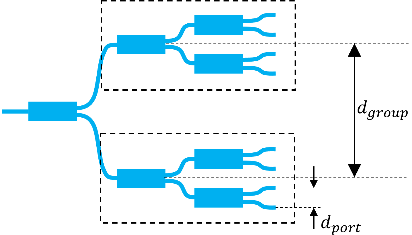
Splitter tree containing 2 waveguide groups, each having 4 output waveguides, where the vertical distances \(d_{port}\) between their output ports is much smaller than the distance \(d_{group}\) between the waveguide groups.
This is done to facilitate our work later on when we will connect the splitter tree and the spiral array. In the splitter tree provided by the Shuksan PDK, the correct distances between all the output ports as well as the positions of all the splitters are automatically calculated depending on the level and the port number within said level. Just like in the splitter tree used in the Optical phased array tutorial, you have the freedom to choose which 1x2 splitter cell to use in the splitter tree. However, instead of setting the amount of output ports, we will have to specify the amount of output ports (or waveguides) per waveguide group, and the amount of waveguide groups. We will also set the vertical distance between ports within a waveguide group (\(d_{port}\)) and the vertical distance between waveguide groups (\(d_{group}\)). The horizontal spacing between the splitter levels is automatically calculated based on the length of the splitter and the waveguide bend radius. The code to generate the splitter tree can be found in the Luceda PDK for SiEPIC Shuksan in luceda_academy/pdks/siepic_shuksan/ipkiss/siepic_shuksan/custom_circuits/splitter_tree/cells.py.
By default, the splitter tree has 4 groups and each group has 4 ports, resulting in 16 output ports in total, but this can obviously be changed to match the number of spirals and grating couplers. The default splitter tree can be visualized by running luceda_academy/pdks/siepic_shuksan/ipkiss/siepic_shuksan/custom_circuits/splitter_tree/cells_test.py
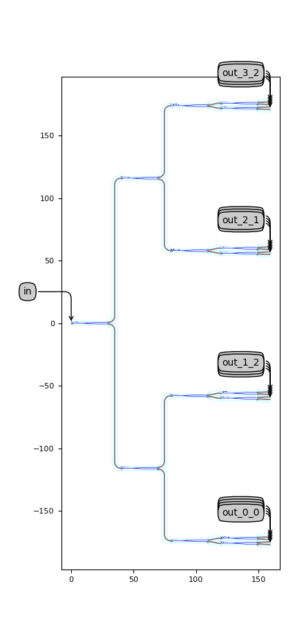
Splitter tree containing four groups of 4 waveguides
Heated spirals matrix
In the spirals provided by the Shuksan PDK, a long waveguide with a fixed length is curved into a circular spiral. This will not only lead to having a lower footprint on chip; when placed below a heater, the spiral structure will also enable a very efficient thermo-optic phase shifter. Contrary to the regular, straight thermo-optic phase shifters, where the heater metal has the same length as the waveguide length, the spiral allows for a doughnut-shaped layout of the heater metal, below which the optical waveguide can circle several times. Since this results in a much shorter and wider heater as compared to the straight one, a much lower heater resistance is achieved and consequently, the driving voltage is greatly reduced.
The spiral is implemented in such a way that for a certain set of layout parameters (such as inner radius and waveguide separation) the angular offset of the inner half circles and the amount of revolutions are automatically calculated to achieve a given spiral waveguide length. The heater width is then automatically adjusted so that it covers all revolutions of the spiral waveguide. An example of a heated spiral is provided in luceda_academy/pdks/siepic_shuksan/ipkiss/siepic_shuksan/custom_circuits/spiral_matrix/cells_test.py and is depicted below. It has a length of 500 micron, an inner radius of 5 micron, and a waveguide separation of 500 nm, yielding a spiral with 6 revolutions and a heater metal that is approximately 6 micron wide.
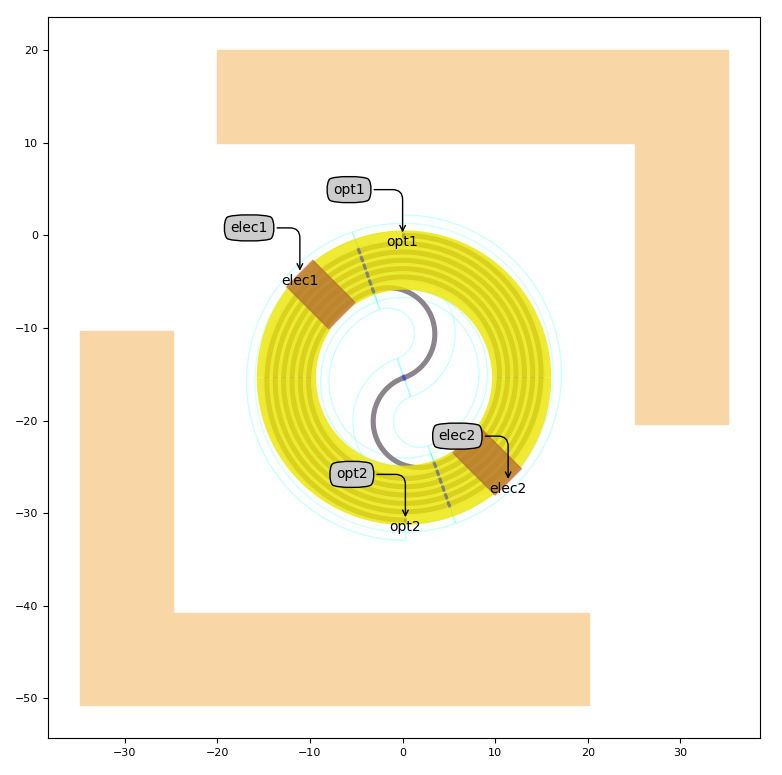
Depiction of a heated spiral containing a 500 micron long waveguide covered by a heater (yellow), 2 M2 metal pads (dark brown) and the OX_OPEN_SI regions (light brown)
As can be seen from the figure, the heater also contains 2 contact pads defined in layer M2 that are opposite to each other but can be rotated under a certain angle (in this case 45 degrees in order to expose the optical ports), giving an additional degree of layouting flexibility to the user.
Finally, it can also be seen that two identical regions of OX_OPEN_SI are placed alongside the spiral, which is done in order to improve thermal isolation to and from its surroundings.
In the picture above, the OX_OPEN_SI has a width of 10 micron as per the design rules of the SiEPIC Shuksan PDK.
Now that we know which spiral we’re going to use as our thermo-optic shifter, we will place a number of copies of this heated spiral in a 2D matrix. The code to generate the 2D matrix is provided in the Shuksan PDK in luceda_academy/pdks/siepic_shuksan/ipkiss/siepic_shuksan/custom_circuits/spiral_matrix/cells.py.
This PCell contains several parameters such as the number of rows and columns, the heated spiral PCell and some layout parameters for the waveguide and electric wire routes. The waveguide routing parameters are needed as we want to route the optical waveguides to the left and right side of the spiral matrix in order to facilitate connecting the spiral matrix to the grating couplers and splitter tree. The same holds true for the electric wire routing parameters as it will greatly facilitate routing the metal pads on the heated spirals towards the bondpads on the full chip. The ground pads of all the heaters are connected to a common ground, meaning only one wire needs to be connected to the ground pad when layouting the full OPA. The bias pads on the heaters are routed partially outside of the spiral region which will also facilitate the eventual routing towards the probe pads on chip when designing the whole OPA. In any case, the default heated spiral matrix can be visualized by running luceda_academy/pdks_sources/siepic_shuksan/siepic_shuksan/custom_circuits/spiral_matrix/cells_test.py.
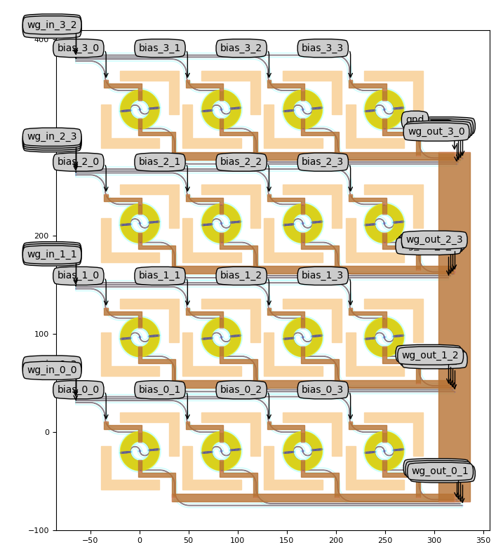
Default heated spiral matrix, showing how the ground pads on the spirals are all connected to a common ground, the bias pads routed further away from the spiral centers and the in- and output waveguides are routed towards the left and right side of the matrix respectively.
Grating couplers matrix
Just like the spirals, the fiber grating couplers are placed in a 2D matrix with the same amount of rows and columns as the spiral matrix. The routing here is simpler, considering there are no metal wires to be routed and only the input waveguides need to be connected (to the spiral matrix). The code to generate the fiber array is provided by the Shuksan PDK in luceda_academy/pdks/siepic_shuksan/ipkiss/siepic_shuksan/custom_circuits/grating_coupler_matrix/cells.py.
A number of parameters describe the grating coupler matrix, the first being the number of rows and columns of the matrix and the grating coupler cell.
Parameters related to the placement of the grating couplers are the horizontal and vertical separation between the grating couplers.
The other parameters are related to the waveguide routing towards the left side of the grating coupler matrix and include the straight buffer length, the bend radius of the waveguides and the waveguide separation.
Another parameter is also added to specify whether you want to route central waveguides further to the left.
By default, this is True, as this will facilitate connecting the grating coupler matrix to the spiral matrix.
The default grating coupler matrix can be visualized by running luceda_academy/pdks/siepic_shuksan/ipkiss/siepic_shuksan/custom_circuits/grating_coupler_matrix/cells_test.py.
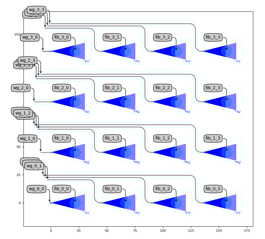
Default grating coupler matrix, showing that the central routing waveguides are extended further to the left than the outer routing waveguides.
OPA1 Layout
Finally, we have arrived at the design of the OPA1 where we place the individual components on the chip and connect them all together. The code to do so is given below:
class OPA1(i3.Circuit):
    """First type of Optical phased array (OPA1) as described in the Shuksan PDK documentation.
    The heaters of the spirals are electrically connected to metal contact pads via electrical wires.
    In this example, the OPA consists of a laser, splitter tree, a 2D matrix of heated spirals and a 2D matrix of
    grating couplers. The heaters are connected to an array of bondpads. This OPA has the following properties:
    - The bondpads are all horizontally aligned with the top of the laser devrec box.
    - The amount of grating couplers is the same as the amount of spirals and both have the same number of
      columns and rows.
    - The amount of columns in the spiral matrix matches the amount of waveguides in a group of output waveguides of the
      splitter tree
    - The amount of rows in the spiral matrix matches the amount of groups in the splitter tree
    - The output waveguides of the splitter tree should be aligned with the input waveguides of the spiral matrix
    The netlist is automatically adapted in order to allow circuit simulations of this component.
    """

    laser = i3.ChildCellProperty(doc="Laser cell")
    splitter_tree = i3.ChildCellProperty(doc="Splitter tree cell")
    spiral_matrix = i3.ChildCellProperty(doc="Heated spiral matrix cell")
    grating_coupler_matrix = i3.ChildCellProperty(doc="Grating coupler matrix cell")
    bond_pad_sep = i3.PositiveNumberProperty(doc="Separation between the bondpads", default=25.0)
    wg_radius = i3.PositiveNumberProperty(doc="Radius of the routed waveguide bends", default=5.0)
    m_width_laser_to_bondpads = i3.PositiveNumberProperty(
        doc="Electric wires width of the laser towards the pads",
        default=20.0,
    )
    m_width_heaters_to_bondpads = i3.PositiveNumberProperty(
        doc="Electric wires width of the heater towards the pads",
        default=8.0,
    )
    m_sep_heaters_spirals = i3.PositiveNumberProperty(
        doc="Separation of the heater electric wires within the spiral array",
        default=3.0,
    )
    m_sep_heaters_to_bondpads = i3.PositiveNumberProperty(
        doc="Separation of the heater electric routes outside of spiral array, towards the bondpads",
        default=5.0,
    )
    n_bondpads = i3.IntProperty(doc="Number of bondpads, calculated from the child cells", locked=True)

    def _default_laser(self):
        return pdk.laser_1270nm()

    def _default_splitter_tree(self):
        return pdk.ShuksanSplitterTree()

    def _default_spiral_matrix(self):
        return pdk.HeatedSpiralMatrix()

    def _default_grating_coupler_matrix(self):
        return pdk.GratingCouplerMatrix()

    def _default_n_bondpads(self):
        return 3 + self.spiral_matrix.n_rows * self.spiral_matrix.n_cols  # 3 extra pads for laser and common ground

    def _default_specs(self):
        ################################################################################################################
        # Retrieve layout parameters of the cells and calculate several layout parameters

        n_rows = self.spiral_matrix.n_rows
        n_cols = self.spiral_matrix.n_cols
        wg_r = self.wg_radius
        m_w = self.spiral_matrix.spiral.contacts_width
        m_w_laser = self.m_width_laser_to_bondpads
        m_pitch = m_w + self.m_sep_heaters_spirals
        m_pitch_to_bpds = self.m_sep_heaters_to_bondpads + self.m_width_heaters_to_bondpads
        spiral_ox_out = self.spiral_matrix.spiral.ox_open_width + self.spiral_matrix.spiral.ox_open_sep

        laser_lay = self.laser.get_default_view(i3.LayoutView)
        laser_shift_x = np.abs(laser_lay.size_info().east - laser_lay.ports["opt1"].x)

        st_ports = self.splitter_tree.get_default_view(i3.LayoutView).ports
        st_lay_dx = np.abs(st_ports["in"].x - st_ports["out_0_0"].x)

        hsm_ports = self.spiral_matrix.get_default_view(i3.LayoutView).ports
        hsm_bias_y = st_ports["out_0_0"].y - hsm_ports["wg_in_0_0"].y + spiral_ox_out - 2 * self.spiral_matrix.wg_radius
        hsm_shift_x_st = np.abs(n_rows * n_cols * m_pitch_to_bpds - st_lay_dx) + self.m_sep_heaters_to_bondpads
        hsm_cc_gnd = 2 * m_w * min(n_rows, 8)
        hsm_dy = np.abs(hsm_ports["wg_out_0_0"].y - hsm_ports[f"wg_out_{n_rows - 1}_{n_cols - 1}"].y)

        gcm_ports = self.grating_coupler_matrix.get_default_view(i3.LayoutView).ports
        gcm_dy = np.abs(gcm_ports["wg_0_0"].y - gcm_ports[f"wg_{n_rows - 1}_{n_cols - 1}"].y)
        gcm_shift_y_hsm = 0.5 * np.abs(hsm_dy - gcm_dy)

        ################################################################################################################
        # place components on their desired location

        specs = [
            i3.Inst("laser", self.laser),
            i3.Inst("st", self.splitter_tree),
            i3.Inst("hsm", self.spiral_matrix),
            i3.Inst("gcm", self.grating_coupler_matrix),
            i3.Inst([f"bp_{bp_i}" for bp_i in range(self.n_bondpads)], pdk.BondPad()),
            i3.Place("laser:opt1", (0.0, 0.0)),
            i3.Place.X("st:in", 0.0, relative_to="laser@E"),
            i3.Place.Y("st:in", 0.0, relative_to="laser@C"),
            i3.Place("hsm:wg_in_0_0", (hsm_shift_x_st, 0.0), relative_to="st:out_0_0"),
            i3.Place("gcm:wg_0_0", (2 * hsm_cc_gnd, gcm_shift_y_hsm), relative_to="hsm:wg_out_0_0"),
        ]

        # Place bp1 relative to the NE corner of laser
        # Horizontally distribute other bondpads to the left and right of bp1 with clearance self.bond_pad_sep
        # Align bondpads
        specs += [
            i3.Place("bp_1@SE", (-0.5 * self.bond_pad_sep, 6 * m_w_laser), relative_to="laser@NE"),
            i3.Place.X("bp_0@E", -self.bond_pad_sep, relative_to="bp_1@W"),
            i3.AlignH([f"bp_{bp_i}" for bp_i in range(self.n_bondpads)]),
        ]
        specs += [
            i3.Place.X(f"bp_{bp_i}@W", self.bond_pad_sep, relative_to=f"bp_{bp_i - 1}@E")
            for bp_i in range(2, self.n_bondpads)
        ]

        ################################################################################################################
        # optical connections between the arrayed components

        specs.append(i3.ConnectBend("laser:opt1", "st:in", bend_radius=wg_r))
        for row in range(n_rows):
            for col in range(n_cols):
                p_i = f"_{row}_{col}"
                specs.append(i3.ConnectBend(f"st:out{p_i}", f"hsm:wg_in{p_i}", bend_radius=wg_r))
                specs.append(i3.ConnectBend(f"hsm:wg_out{p_i}", f"gcm:wg{p_i}", bend_radius=wg_r))

        ################################################################################################################
        # electrical bias connections between spirals and intermediate ports

        intermediate2_ports = []
        trace_template_m_w = pdk.M2WireTemplate().Layout(m_width=m_w).cell

        for row in range(n_rows):
            for col in range(n_cols):
                bias_port_x_out = laser_shift_x + (n_cols * row + col + 1) * m_pitch_to_bpds
                bias_port_y_out = hsm_ports[f"wg_in_{row}_0"].y + hsm_bias_y + col * m_pitch
                specs.append(
                    i3.ConnectElectrical(
                        f"hsm:bias_{row}_{col}",
                        i3.ElectricalPort(
                            name=f"hsm_bias_{row}_{col}_intermediate1",
                            position=(bias_port_x_out, bias_port_y_out),
                            trace_template=trace_template_m_w,
                            layer=pdk.TECH.PPLAYER.M2_ROUTING,
                        ),
                        start_angle=90.0,
                        end_angle=0.0,
                        trace_template=trace_template_m_w,
                    )
                )

                intermediate2_ports.append(
                    i3.ElectricalPort(
                        name=f"hsm_bias_{row}_{col}_intermediate2",
                        position=(bias_port_x_out, bias_port_y_out - m_w / 2.0),
                        angle=90.0,
                    ),
                )

        ################################################################################################################
        # electrical bias connections between intermediate ports and bondpads

        fanout_connect_position = (
            intermediate2_ports[0].x,
            intermediate2_ports[-1].y,
        )
        specs.append(
            i3.ConnectElectricalBundle(
                connections=[(intermediate2_ports[i], f"bp_{i + 2}:m_pin_bottom") for i in range(n_rows * n_cols)],
                connection_name="bp_to_intermediate",
                trace_template=pdk.M2WireTemplate().Layout(m_width=self.m_width_heaters_to_bondpads).cell,
                start_fanout=i3.SBendFanout(
                    reference=intermediate2_ports[0],
                    end_position=fanout_connect_position,
                ),
                end_fanout=i3.SBendFanout(
                    reference="bp_2:m_pin_bottom",
                    end_position=fanout_connect_position,
                ),
                end_straight=self.m_width_laser_to_bondpads + self.m_sep_heaters_to_bondpads,
                min_gap=self.m_sep_heaters_to_bondpads,
            )
        )

        ################################################################################################################
        # connect common ground wire to the bondpad

        specs.append(
            i3.ConnectElectrical(
                "hsm:gnd",
                f"bp_{self.n_bondpads - 1}:m_pin_bottom",
                start_angle=90.0,
                end_angle=-90.0,
                control_points=[i3.H(-(n_cols - 1) * m_pitch_to_bpds, relative_to="hsm@N")],
                trace_template=pdk.M2WireTemplate().Layout(m_width=hsm_cc_gnd).cell,
            )
        )

        ################################################################################################################
        # connect laser to the bondpads

        specs.append(
            i3.ConnectElectricalBundle(
                connections=[
                    ("laser:elec2_n", "bp_1:m_pin_bottom"),
                    ("laser:elec1_p", "bp_0:m_pin_bottom"),
                ],
                connection_name="laser_to_bp",
                trace_template=pdk.M2WireTemplate().Layout(m_width=m_w_laser).cell,
                start_fanout=i3.ManhattanFanout(
                    output_direction=i3.NORTH,
                ),
                end_fanout=i3.ManhattanFanout(
                    output_direction=i3.WEST,
                ),
                min_gap=m_w_laser,
                start_straight=m_w_laser,
                end_straight=m_w_laser,
            )
        )
        return specs

    def _default_exposed_ports(self):
        ports = {}
        for row in range(self.spiral_matrix.n_rows):
            for col in range(self.spiral_matrix.n_cols):
                ports[f"gcm:fib_{row}_{col}"] = f"fib_{row}_{col}"
        ports["bp_0:m_pin_top"] = "laser_p"
        ports["bp_1:m_pin_top"] = "laser_n"
        for row in range(self.spiral_matrix.n_rows):
            for col in range(self.spiral_matrix.n_cols):
                bp_i = row * self.spiral_matrix.n_cols + col + 2
                ports[f"bp_{bp_i}:m_pin_top"] = f"bias_spiral_{row}_{col}"
        ports[f"bp_{self.n_bondpads - 1}:m_pin_top"] = "common_gnd"
        return ports

    ####################################################################################################################
    # Adapt netlist to allow for simulations

    class Netlist(i3.NetlistFromLayout):
        def _generate_netlist(self, netlist):
            netlist = super()._generate_netlist(self)
            instances = copy.copy(netlist.instances)
            for instname in instances:
                instref = netlist.instances[instname].reference
                if is_electrical_cell(instref.cell):
                    netlist.instances.pop(instname)
                    remove_nets = set()
                    for net in netlist.nets.values():
                        for term in net.terms:
                            if isinstance(term, InstanceTerm) and term.instance.name == instname:
                                remove_nets.add(net.name)
                    for net_name in remove_nets:
                        netlist.nets.pop(net_name)
            netlist += i3.ElectricalNet([netlist["hsm"].terms["gnd"], netlist["common_gnd"]], name="common_gnd")
            netlist += i3.ElectricalNet([netlist["laser"].terms["elec1_p"], netlist["laser_p"]], name="laser_p")
            netlist += i3.ElectricalNet([netlist["laser"].terms["elec2_n"], netlist["laser_n"]], name="laser_n")
            for row in range(self.spiral_matrix.n_rows):
                for col in range(self.spiral_matrix.n_cols):
                    netlist += i3.ElectricalNet(
                        [
                            netlist["hsm"].terms[f"bias_{row}_{col}"],
                            netlist[f"bias_spiral_{row}_{col}"],
                        ],
                        name=f"bias_spiral_{row}_{col}",
                    )
            return netlist
This cell contains the following layout parameters:
The cells for the splitter tree, heated spiral matrix and grating coupler matrix
The bend radius for the waveguides
The number of bondpads in the bondpad array
The pitch of the bondpad array (which is connected via metal tracks to the heated spiral array)
The width of the metal routes to the bondpad array: from the laser, from the heated spiral array
The separation between the metal routes inside and outside the heated spiral array
Next to the layout, we also need to redefine the netlist of the OPA.
Indeed, just like in the Optical phased array tutorial, we have to remove the metal components (the bondpads and metal tracks) of the OPA1 from the netlist to enable the circuit simulations as these components don’t have a compact model associated with them.
However, since we define all the electric input ports for external probing in the circuit simulation at the bondpads, we need to ‘link’ the bondpads to the bias pads and the common ground of the heated spiral matrix as well as the two contact pads of the laser.
This is done in the OPA1 netlist through i3.ElectricalNet as can be seen from the code.
The OPA1 can now be simulated with CAPHE, which will be discussed in the next section.
Coming back to the OPA1 layout, we need to ensure that several parameters of the splitter tree, heated spiral matrix and grating coupler matrix are the same in order for the waveguide routing to work properly:
The number of heated spiral columns should match the number of waveguides within a group of the splitter tree, whereas the number of heated spiral rows should match the number of groups.
The waveguide separation and the vertical separation within the heated spiral matrix should match the vertical distance between, respectively, the splitter tree waveguides within a group and between the splitter tree groups.
The number of columns and rows in the heated spiral matrix and in the grating coupler matrix should match, and they should all be powers of 2.
This is shown in the following code:
import siepic_shuksan.all as pdk
import matplotlib.pyplot as plt
import numpy as np

import ipkiss3.all as i3
from opa1.cells import OPA1, OPAWithFloorplan

########################################################################################################################
# Parameters for the layout and the simulation
########################################################################################################################

# Simulation parameters
t_start = 0.0  # start time
delta_t = 1.0e-11  # time steps
n_points = 2**15  # number of time steps in the simulation
t_stop = (n_points - 1) * delta_t  # stop time

# Layout parameters
n_rows = 4
n_cols = 4
spiral_sep_x = 83.0
spiral_sep_y = 140.0 if n_cols > 4 else 116.0
spiral_length = 500.0
spiral_contacts_width = 4.0
waveguide_separation = 2.0


########################################################################################################################
# OPA layout and gds export
########################################################################################################################

# Instantiate the subcomponents of the OPA
spiral = pdk.SpiralCircularWithHeater(spiral_length=spiral_length, contacts_width=spiral_contacts_width)
laser = pdk.laser_1270nm()
heated_spiral_matrix = pdk.HeatedSpiralMatrix(
    spiral=spiral,
    n_rows=n_rows,
    n_cols=n_cols,
    spiral_sep_x=spiral_sep_x,
    spiral_sep_y=spiral_sep_y,
    wg_sep=waveguide_separation,
)
splitter_tree = pdk.ShuksanSplitterTree(
    n_wgs_per_wg_group=n_cols,
    n_wg_groups=n_rows,
    spacing_y_ports=waveguide_separation,
    spacing_y_groups=spiral_sep_y,
)
grating_coupler_matrix = pdk.GratingCouplerMatrix(
    n_rows=n_rows,
    n_cols=n_cols,
)

# Instantiate the OPA using the components defined above and plot the layout
opa = OPA1(
    name="OPA1",
    laser=laser,
    splitter_tree=splitter_tree,
    spiral_matrix=heated_spiral_matrix,
    grating_coupler_matrix=grating_coupler_matrix,
)
layout = opa.Layout()
layout.visualize()
layout.to_canvas()

# Export the layout of the OPA with chip floor plan to GDS
OPAWithFloorplan(name="OPA1WithFloorplan", opa=opa).Layout().write_gdsii(f"opa1_{n_rows}x{n_cols}_with_floorplan.gds")
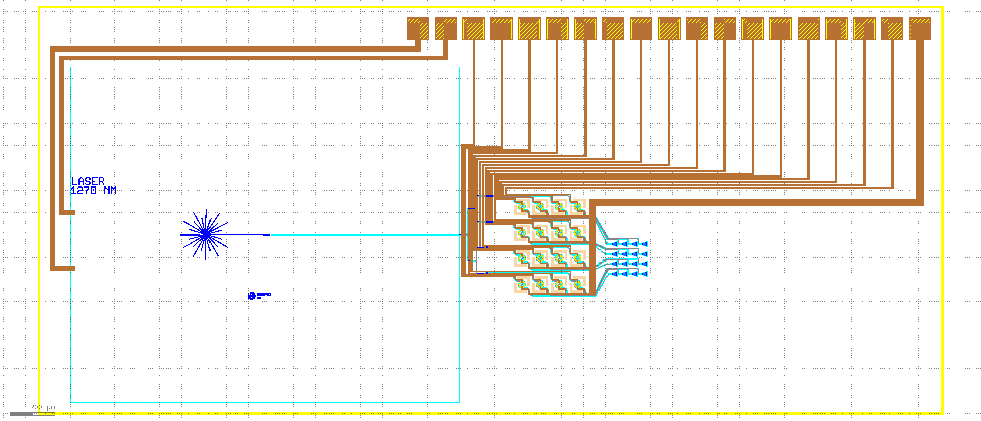
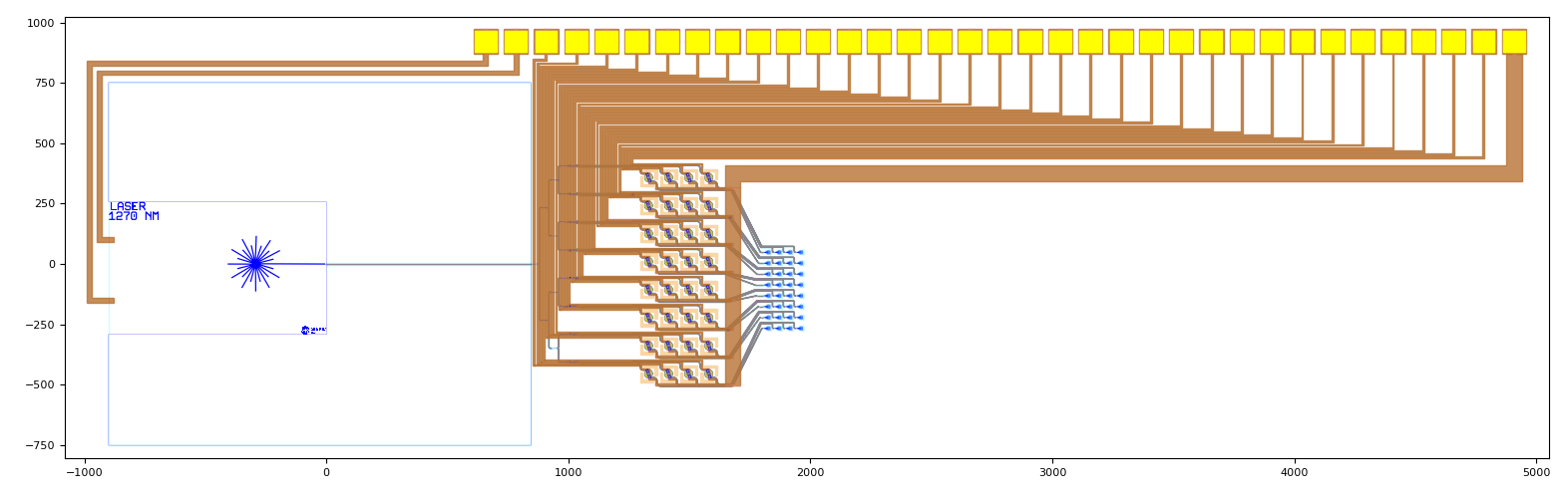
With this in mind, we now define the desired splitter tree, heated spiral matrix and grating coupler matrix. These components are then passed on as child cell parameters to the OPA1 cell. The waveguide connections between the components as well as the metal routing are then all placed automatically within the OPA1 cell. The code is written in such a way that when you change the number of rows and columns of the matrices, it will automatically adapt the placement of the cells, waveguide connectors and electric routes so that these components don’t overlap internally. Now that the OPA1 cell is instantiated, its layout can be visualized with Luceda IPKISS as shown below for when OPA1 has, respectively, a 4x4 and an 8x4 matrix of spirals and grating couplers:
Layout of the OPA1 containing 4 rows and 4 columns of heated spirals and grating couplers.
Layout of the OPA1 containing 8 rows and 4 columns of heated spirals and grating couplers.
If we want to send this design to the SiEPICfab foundry, we also need to add the floorplan of the chip, which is done with the following code:
class OPAWithFloorplan(i3.Circuit):
    """User defined OPA placed on the chip floor plan, whose size is adapted to the OPA size"""

    opa = i3.ChildCellProperty(doc="OPA cell")

    def _default_opa(self):
        return OPA1()

    def _default_specs(self):
        opa_lay = self.opa.get_default_view(i3.LayoutView)
        width = opa_lay.size_info().east - opa_lay.size_info().west + 100.0
        height = opa_lay.size_info().north - opa_lay.size_info().south + 100.0
        x_loc = 0.5 * (opa_lay.size_info().east + opa_lay.size_info().west)
        y_loc = 0.5 * (opa_lay.size_info().north + opa_lay.size_info().south)
        return [
            i3.Inst("opa", opa_lay),
            i3.Inst("floorplan", pdk.Floorplan(width=width, height=height)),
            i3.Place("floorplan", (x_loc, y_loc)),
        ]
This cell will ensure that the size and location of the chip floorplan is automatically adapted to the size and location of the OPA.
The OPA with chip floorplan will then be exported to a GDS file by running OPAWithFloorplan(opa=opa).Layout().write_gdsii() as is done in example_routed_opa_shuksan.py.
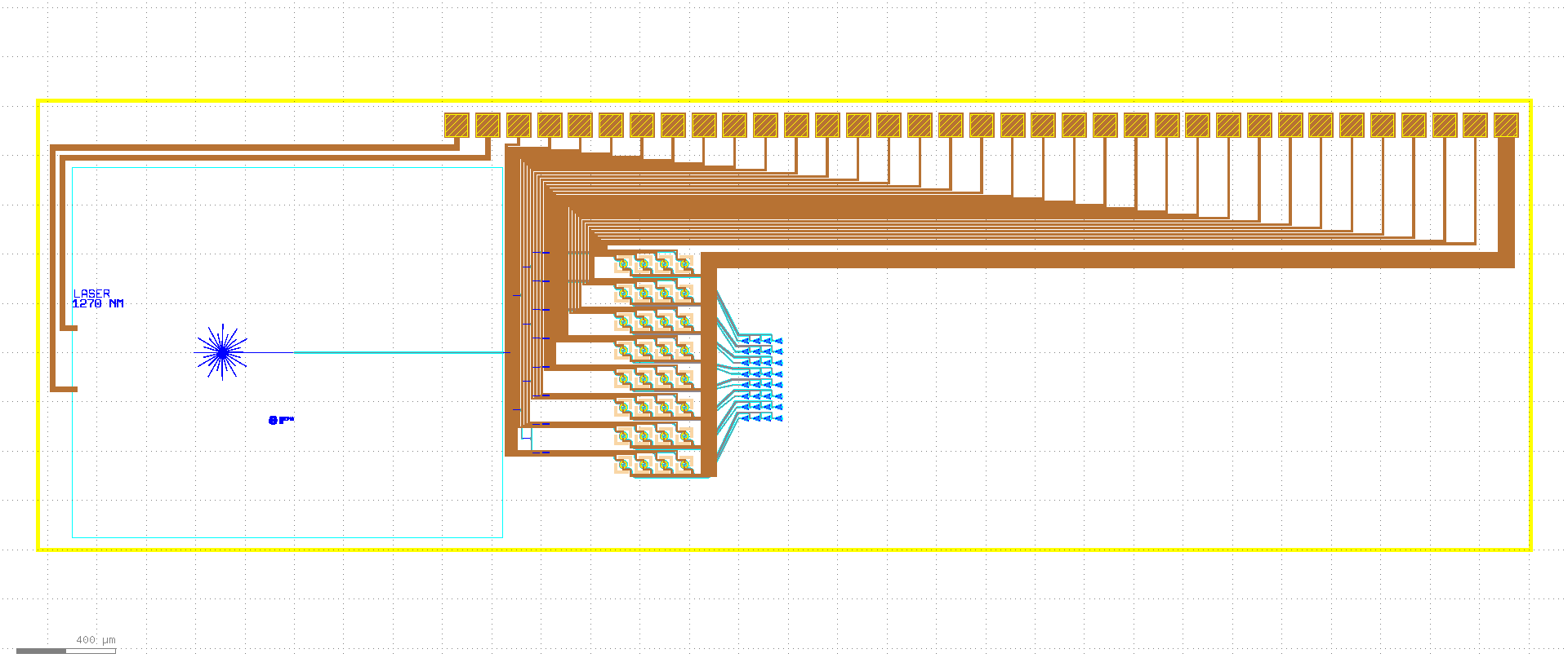
Below, you can see the GDS of an OPA with a 4x4 and an 8x4 matrix of spirals and grating couplers.
GDS of the OPA1 containing 4 rows and 4 columns of heated spirals and grating couplers.
GDS of the OPA1 containing 8 rows and 4 columns of heated spirals and grating couplers.
OPA1 Simulation
In the second part of the example_routed_opa_shuksan.py code, we set up the simulation test bench for the OPA1:
laser_probe = i3.FunctionExcitation(
    port_domain=i3.ElectricalDomain,
    excitation_function=pdk.create_step_function(t_start=0.0, t_rise=delta_t, amplitude=1.5),
)
gnd_probe = i3.FunctionExcitation(
    port_domain=i3.ElectricalDomain,
    excitation_function=pdk.create_step_function(t_start=0.0, t_rise=delta_t, amplitude=0.0),
)
child_cells = {"opa": opa, "hsm_gnd": gnd_probe, "laser_probe": laser_probe, "laser_gnd": gnd_probe}
links = [("opa:common_gnd", "hsm_gnd:out"), ("opa:laser_p", "laser_probe:out"), ("opa:laser_n", "laser_gnd:out")]
for row in range(n_rows):
    for col in range(n_cols):
        nom = 2.0 * (row * n_cols + col) / (n_rows * n_rows) + 1.0
        bias_port = f"bias_spiral_{row}_{col}"
        child_cells[bias_port] = i3.FunctionExcitation(
            port_domain=i3.ElectricalDomain,
            excitation_function=pdk.create_step_function(t_start=0.0, t_rise=t_stop * nom, amplitude=1.0),
        )
        child_cells[f"fib_{row}_{col}"] = i3.Probe(port_domain=i3.OpticalDomain)
        links.append((f"opa:{bias_port}", f"{bias_port}:out"))
        links.append((f"opa:fib_{row}_{col}", f"fib_{row}_{col}:in"))
opa_test_bench_cm = i3.ConnectComponents(child_cells=child_cells, links=links).CircuitModel()
result = opa_test_bench_cm.get_time_response(t0=0.0, t1=t_stop, dt=delta_t, center_wavelength=1.26809004)
times = result.timesteps

plt.figure(num=1)
for row in range(n_rows):
    for col in range(n_cols):
        voltage = result[f"bias_spiral_{row}_{col}"].real
        plt.plot(result.timesteps * 1e9, voltage, "o-", label=f"bias_spiral_{row}_{col}")
plt.xlabel("times [ns]", fontsize=15)
plt.ylabel("Voltage [V]", fontsize=15)
plt.legend(fontsize=12)

plt.figure(num=2)
plt.subplot(121)
for row in range(n_rows):
    for col in range(n_cols):
        probe = f"fib_{row}_{col}"
        plt.plot(result.timesteps * 1e9, 1e3 * np.abs(result[probe]) ** 2, "o-", label=f"fib_{row}_{col}")
plt.xlabel("times [ns]", fontsize=15)
plt.ylabel("Power [mW]", fontsize=15)
plt.legend(fontsize=12)

plt.subplot(122)
for row in range(n_rows):
    for col in range(n_cols):
        probe = f"fib_{row}_{col}"
        plt.plot(result.timesteps * 1e9, np.unwrap(np.angle(result[probe])), "o-", label=f"fib_{row}_{col}")
plt.xlabel("times [ns]", fontsize=15)
plt.ylabel("Phase [rad]", fontsize=15)
plt.legend(fontsize=12)
plt.show()
We define the electric sources for the laser and the heated spirals.
The voltage source for the laser is constant during the whole simulation at \(1.5\,V\), yielding a laser power of approximately \(1.5\,mW\), while the voltage sources for the heaters vary linearly over time, with a speed different for each heated spiral.
We also define the grounds for the laser as well as the common ground of the heated spiral matrix.
Next to the voltage source, we define optical probes that ‘measure’ the light coming from the grating couplers of the grating coupler matrix.
This will enable us to see how the phases of the light beams change as the voltages on the heaters are varied.
All of the probes and voltage sources are then connected through i3.ConnectComponents.
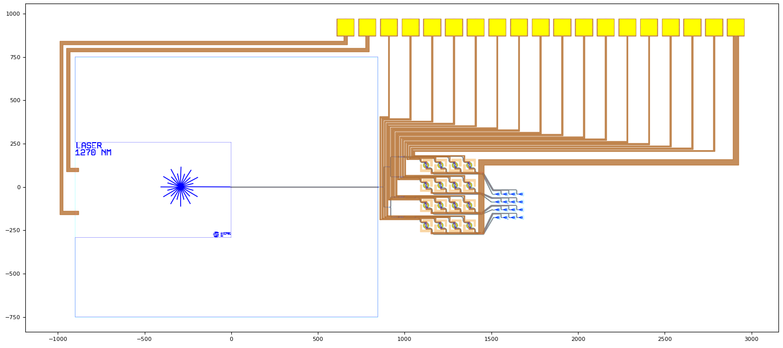
The electric and optical ports as well as the bias voltages for the heated spirals associated with this simulation are visualized below.
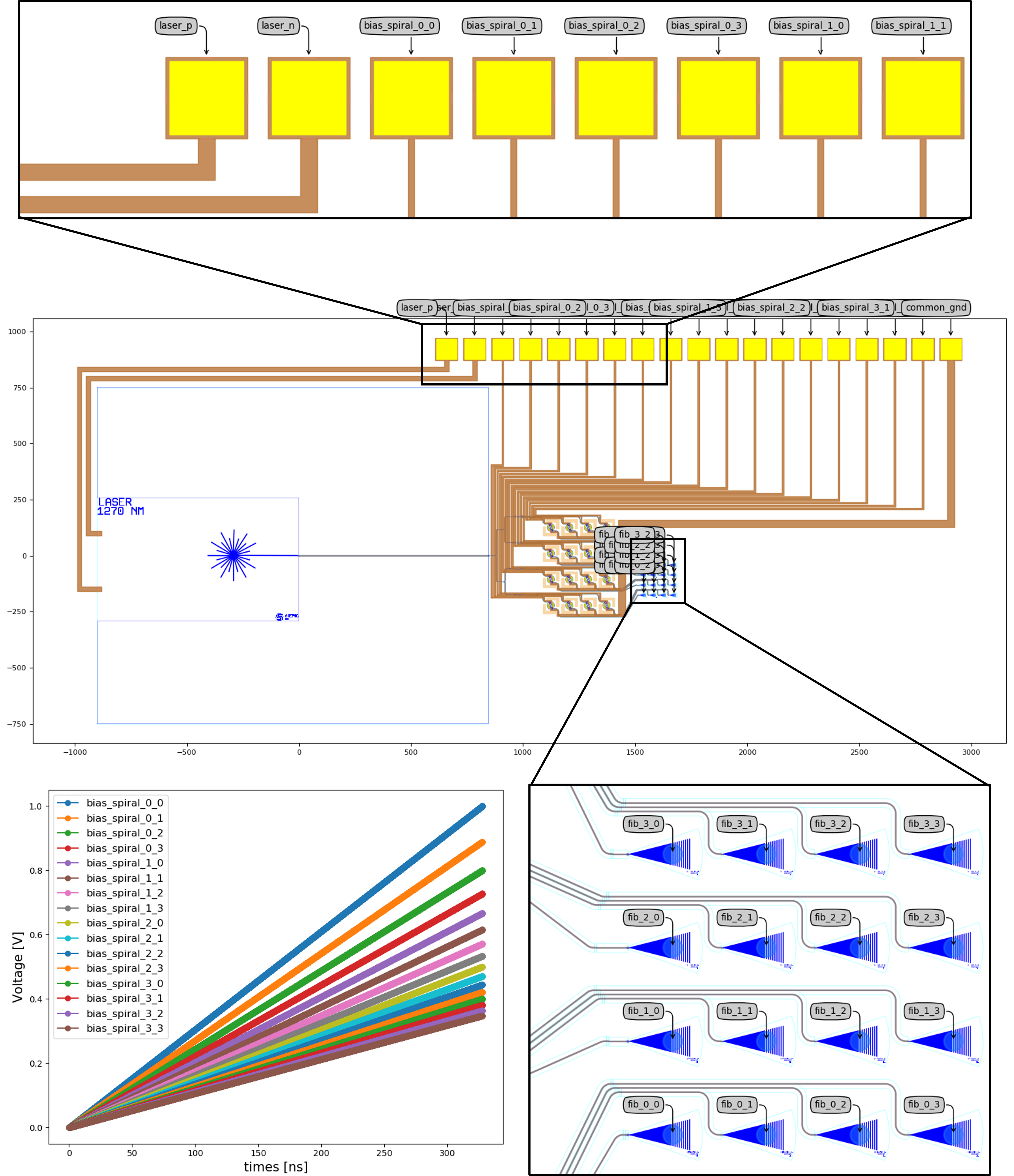
Layout of OPA1 indicating the grating coupler matrix (bottom right inset) and several electric probe pads (top inset). We also plot the bias voltage as a function of time for each heated spiral in the bottom left picture.
Finally, we define the simulation wavelength at \(1.26809004\,\mu m\) for it to match the emitted laser wavelength for the given voltage applied to the laser. The laser model calculates the actual emitted wavelength for a given voltage bias and temperature, and takes into account the offset with the simulation wavelength. Any constant optical frequency offset will result in a linearly increasing phase over time. Since we only want to calculate the phases induced by the voltages on the heated spirals, we want this frequency offset as small as possible in order to not skew the simulation results. In this tutorial, we manually calculate the emitted laser wavelength for the given input parameters and set the simulation wavelength accordingly, but this process can be automated. The simulation results are plotted below:
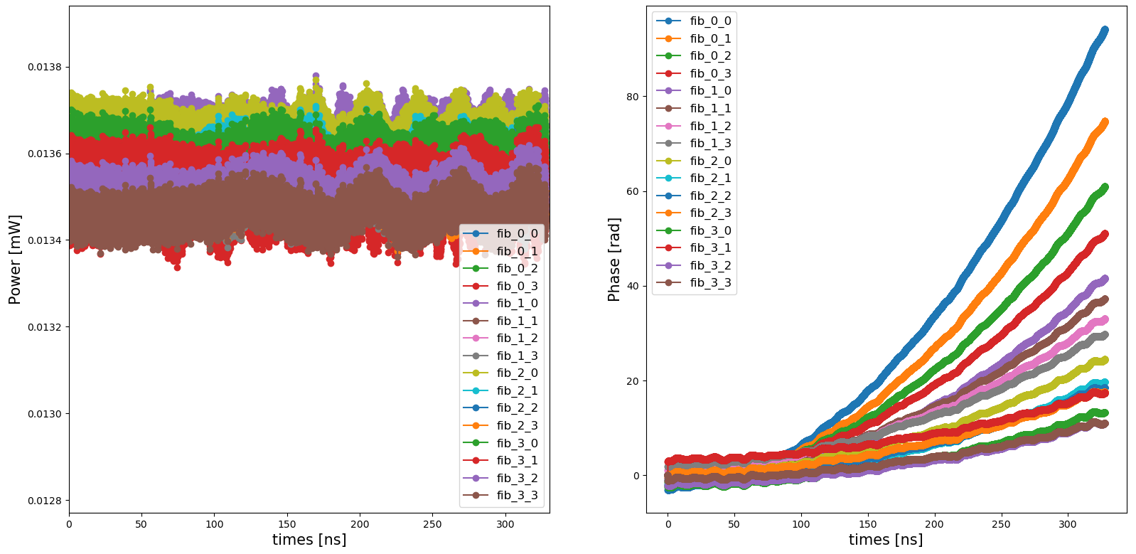
Simulation of the OPA1 containing 4 rows and 4 columns of heated spirals and grating couplers. In the left picture, we look at the power levels of the emitted beams from the grating couplers, while in the right picture, the phase of those emitted beams are plotted, both as a function of time.
We can see that as the voltages vary linearly over time, the phase of the emitted light beam change quadratically over time, as is to be expected from heater based phase shifters. Since the laser model takes into account both the relative intensity noise as well as the phase noise, the emitted powers and phases display a certain level of noise as can be seen from the plots. This can be useful to evaluate the beam steering performance in the presence of these noise terms, but this is outside the scope of this tutorial.