2. Electro-optic phase modulator
In this section, we will discuss how to implement the layout and the circuit model of the high-speed electro-optic phase modulator (EOPM). While there are many physical processes one can employ to achieve phase modulation, we will focus here on carrier depletion. In carrier depletion-type EOPMs, the waveguide carrying the optical wave has a p-n junction.
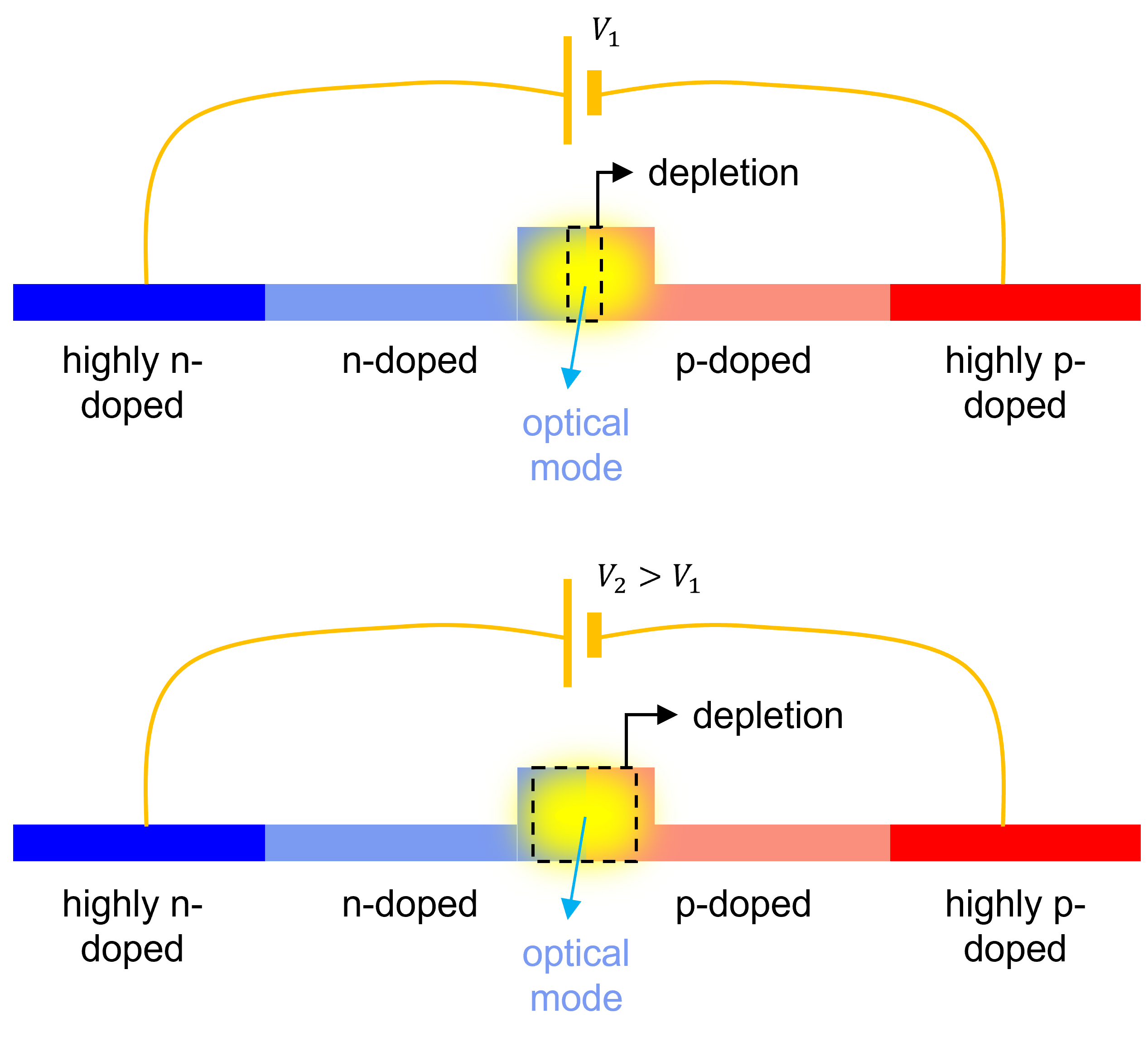
Principle of carrier depletion: a changing bias voltage changes the depletion region or carrier density in the region that overlaps with the waveguide mode, thus altering the mode’s effective index and consequently, its phase.
Between the p- and n-doped regions, there is a region called a depletion region, where the excess carriers have been diffused away. As it can be seen on the figure, the waveguide core overlaps with this region. By applying a reverse voltage, the size of the depletion region increases. In other words, by varying the reverse bias, the carrier density in the waveguide is varied as a result. Since the carrier density affects the refractive index of the waveguide material through the plasma-dispersion effect, a varying reverse bias voltage will thus result in a modulation of the effective index the optical wave experiences. This, in turn, modulates the phase experienced by the optical wave as it propagates along the p-n junction.
In this tutorial, we focus on Si-based carrier depletion EOPMs, although they can be realized in other material platforms as well, such as InP. We will now look at how to properly layout this device so that when we have it fabricated in a Si foundry, it will operate properly. The Si process used for the design relies on the SiFab demo PDK provided by Luceda as part of Luceda Academy. However, this tutorial can be easily retargeted to design modulators for your foundry of choice.
2.1. Layout
We can split the layout of a phase modulator into two parts:
an optical part, that covers the necessary layers to define the undoped waveguide, and
an electrical part, that covers the necessary layers to properly dope the waveguide and provide electrical contact.
2.1.1. Optical Waveguide
The optical part controls the layers to etch in the silicon in order to create a waveguide where a mode can propagate.
The waveguide is a rib waveguide, SiRibWaveguideTemplate, and its layout is controlled by the core_width and rib_width properties.
from si_fab import all as pdk
from ipkiss3 import all as i3

wav_length = 10.0

undoped_template = pdk.SiRibWaveguideTemplate().Layout(core_width=0.45, cladding_width=8.0).cell
undoped_waveguide = i3.Waveguide(trace_template=undoped_template).Layout(shape=[(0.0, 0.0), (wav_length, 0.0)])
undoped_waveguide.visualize(annotate=True)
undoped_waveguide_xs = undoped_waveguide.cross_section(cross_section_path=i3.Shape([(1.0, -8.0), (1.0, 8.0)]))
undoped_waveguide_xs.visualize()
The top- and cross-section views are shown below for reference:
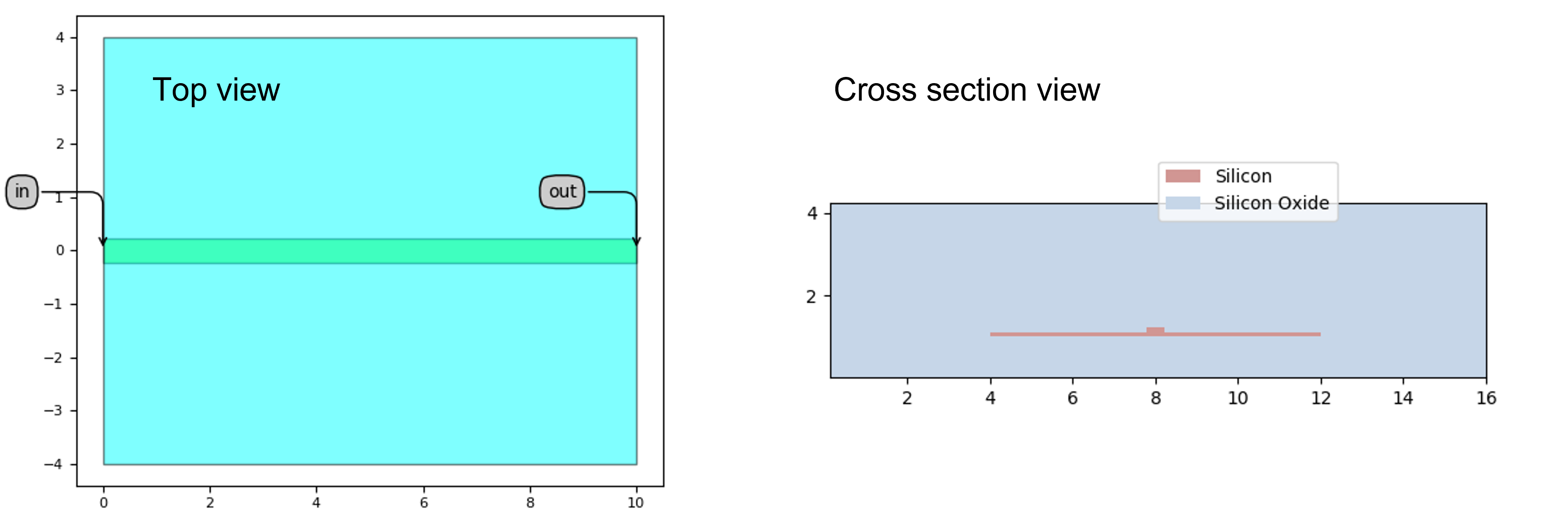
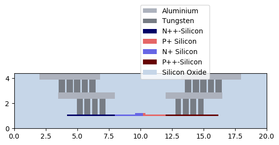
Top view (left) and cross section view (right) of the rib waveguide
As it can be seen, we only need two layers for this waveguide: one layer to define the core of the waveguide and one layer to define the region outside where the silicon is (partially) etched. Now we need to dope this structure to realize the carrier depletion functionality and this will be touched upon in the next section.
2.1.2. Electrical contact
The modulation happens because of the plasma dispersion effect around the junction.
The electrical characteristics of the junction are controlled by the doping profile as a function of position in the waveguide cross section.
SiFab has four possible doping levels: N, P, NPLUS and PPLUS.
Each of these has its equivalent layer: i3.TECH.i3.PPLAYER.N, i3.TECH.i3.PPLAYER.P, i3.TECH.PPLAYER.NPLUS and i3.TECH.PPLAYER.PPLUS.
By default, the junction is exactly in the middle of the waveguide.
If asymmetric doping profiles are used, the junction can be offset by using the junction_offset property.
The width of the p-doped and n-doped layers are set by p_width and n_width.
The offset of the highly doped regions are set by pplus_offset and nplus_offset for p-type and n-type doping, respectively.
Finally, electrical contacts need to be made between those highly doped regions and the metal layers on top, otherwise we won’t be able to generate a voltage difference over the p-n junction. This is done through contact vias between the highly doped regions and the first metal layer M1 of the SiFab process. In particular, these contact vias are made small and are arranged in an array spanning the whole contact region. This will make sure the electrical contact is uniform over the whole modulator device. This array is described by two parameters:
the pitch contact offset, that determines how far the vias are located from the center of the p-n junction, and
the number of contact rows, that determines how many via rows will be used for contacting the doped regions.
Since a via array is required for both the p and n-doped regions, we end up with four properties: p_contact_offset and p_contact_rows for the p-doped regions and n_contact_offset and n_contact_rows for the n-doped regions.
We also then end up with two M1 shapes, one that overlaps with the vias connected to the p-doped region and one that overlaps with the vias connected to the p-doped region.
But considering we assume them to be symmetrically placed relative to the center of the waveguide, we only have two properties here: the width of the M1 layers, m1_width, and the offset between the M1 layer and the center of the waveguide, m1_offset.
Finally, a connection needs to be made between metal layers M2 and M1 through another set of contact vias.
While M1 is the metal layer that connects with the highly doped regions of the p-n junction, M2 is the metal layer that can be exposed for contact with external probes or electric circuitry.
Thus we need another set of contact vias, this time between the layers M1 and M2.
Just like for the M1 shapes, the M2 shapes are placed symmetrically around the center of the waveguide and so are the vias connecting M1 and M2.
As such, the relevant parameters are the width m2_width and offset m2_offset of the M2 shape, the number of via contact rows, n_o_via_row, the distance between adjacent vias, via_pitch and the distance between the via array and the center of the waveguide, via_offset.
The layouting in all these layers is provided by the pdk.PhaseShifterWaveguide() PCell of the SiFab PDK, so you only need to set the values of the properties as demonstrated below:
phase_shift_waveguide = pdk.PhaseShifterWaveguide(
    core_width=0.45,
    rib_width=8.0,
    via_pitch=0.7,
    length=wav_length,
)
phase_shift_waveguide_lv = phase_shift_waveguide.Layout()
phase_shift_waveguide_lv.visualize(annotate=True)
phase_shift_waveguide_xs = phase_shift_waveguide_lv.cross_section(
    cross_section_path=i3.Shape([(1.0, -8.0), (1.0, 8.0)]),
)
phase_shift_waveguide_xs.visualize()
The top- and cross section views of this section are again shown below for reference:
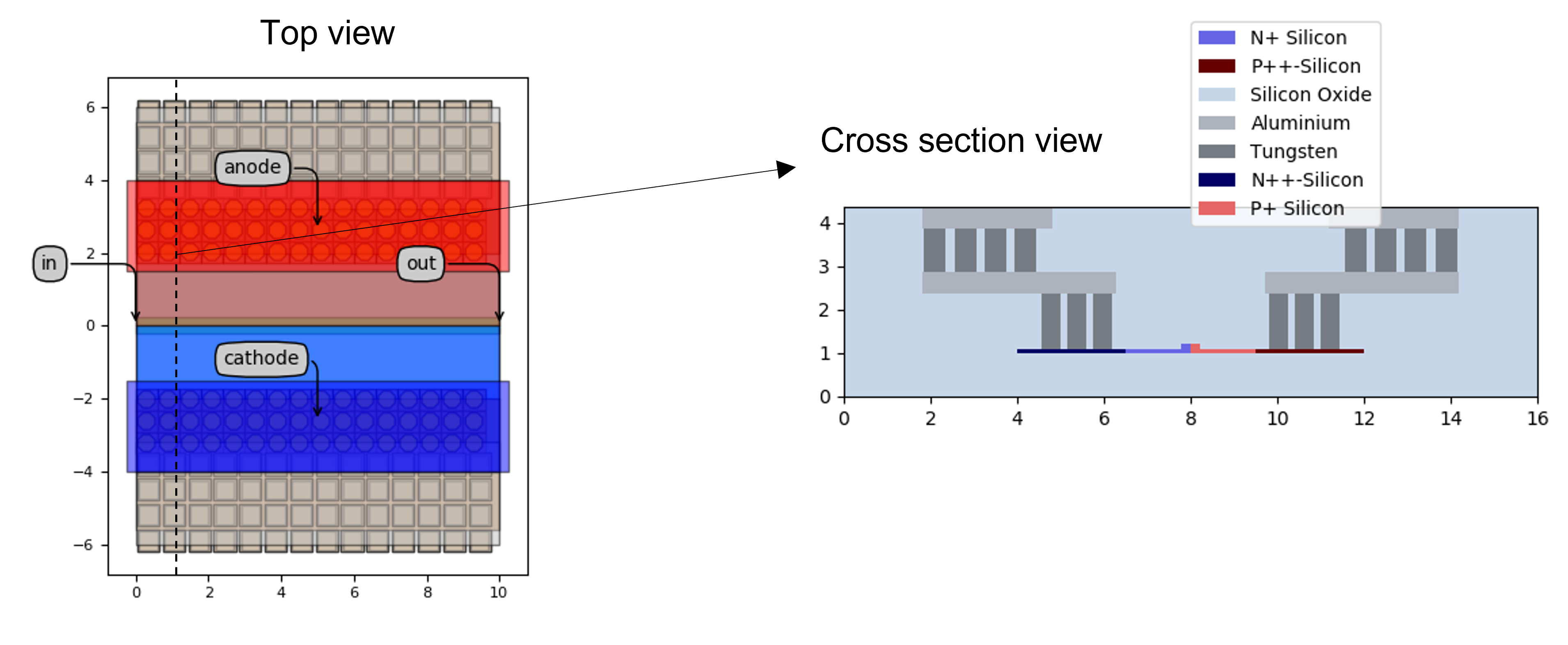
Top view (left) and cross section view (right) of the fully doped rib waveguide, including the metal layers and via arrays.
Now that the layout of the active waveguide has been implemented, we can continue with implementing the actual model of the device.
2.2. Model
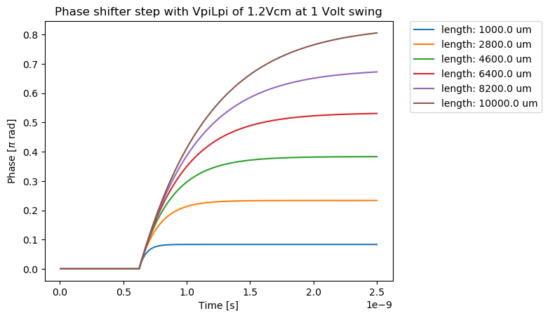
The phase modulator is modeled using a \(V_{\pi}L_{\pi}\) model that is associated with a time constant \(\tau\). Usually, \(V_{\pi}L_{\pi}\) is determined by the reverse bias and the doping profile of the junction, as well as by the temperature. Its value can be obtained through device level simulations or measurements. \(\tau\) is usually dominated by the \(RC\) constant associated with the capacitance of the phase shifter and the driver output resistance. Both \(\tau\) and \(V_{\pi}L_{\pi}\) need to be obtained through measurements or simulations and are not calculated by Luceda IPKISS. It should be stressed that this model is only accurate for relatively short modulator lengths of up to a few hundred microns, as for longer modulator lengths, the device behaves increasingly like a distributed circuit rather than a lumped element. In that case, the simplified description with time constant \(\tau\) will break down and more detailed models that treat the electric signal as a travelling wave need to be implemented.
In SiFab, a simple time constant model has been implemented whereby we take into account how \(\tau\) changes with modulator length. In particular, this is done as follows, considering the \(RC\) constant is the dominating factor:
with \(L_m\) the modulator length, \(C_m\) the capacitance per unit length and \(R_m\) the modulator resistance. The dynamics are then taken into account through the following differential equation that links the voltage over the p-n junction, \(V_j(t)\) with the input voltage \(V_{in}(t)\):
And hence, the total phase change experienced by the optical wave due to the applied voltage is given by
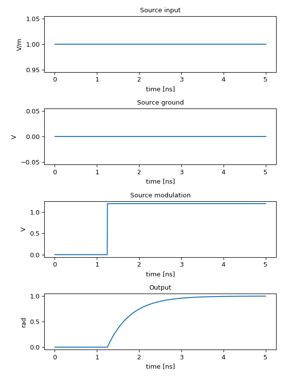
In SiFab, we provide a simulation recipe simulate_phaseshifter which allows us to experiment with the dynamics of the phase modulator.
from si_fab import all as pdk
from si_fab.components.phase_shifter.simulation.simulate import simulate_phaseshifter
import matplotlib.pyplot as plt
import numpy as np
import os

# Phase Shifter
name = "simple_step"
results_array = []
length = 1e4
ps_waveguide = pdk.PhaseShifterWaveguide(
    length=length,
    core_width=0.45,
    rib_width=8.0,
    junction_offset=-0.1,
)
vpi_lpi = 1.2
capacitance = 1.1e-15  # F/um
resistance = 50
tau = ps_waveguide.length * capacitance * resistance
ps_waveguide.CircuitModel(vpi_lpi=vpi_lpi, tau=tau)


results = simulate_phaseshifter(
    cell=ps_waveguide,
    nsteps=1000,
    dt=5e-12,
    step_amplitude=vpi_lpi,
    center_wavelength=1.5,
    debug=False,
)


def phase_unwrap_normalize(optical_out):
    # Unwrap
    phase = np.unwrap(np.angle(optical_out))
    # Normalize (remove phase jump caused by length of waveguide)
    phase_delay = phase[phase != 0.0][0]
    phase[phase == 0.0] = phase_delay
    return (phase - phase_delay) / np.pi


outputs = ["optical_in", "gnd", "vsrc_mod", "optical_out"]
titles = ["Source input", "Source ground", "Source modulation", "Output"]
process = [np.real, np.real, np.real, phase_unwrap_normalize]
ylabels = ["V/m", "V", "V", "rad"]
fig, axs = plt.subplots(nrows=len(outputs), ncols=1, figsize=(6, 8))

for ax, pr, out, ylabel, title in zip(axs, process, outputs, ylabels, titles):
    data = pr(results[out][1:])
    ax.set_title(title)
    ax.plot(results.timesteps[1:] * 1e9, data, label=f"length: {length}")
    ax.set_ylabel(ylabel)
    ax.set_xlabel("time [ns]")

plt.tight_layout()
fig.savefig(os.path.join(f"{name}.png"), bbox_inches="tight")
plt.show()
plt.close(fig)
2.3. Test your knowledge
Exercise 1
Copy
topical_training/mzm/explore_phaseshifter/explore_electrical.py.Try to replicate the following cross-section.
Exercise 2
Copy
topical_training/mzm/explore_phaseshifter/explore_electrical.py.Sweep the length of the phase shifter and explore the compromise between speed and modulation amplitude of the phase.