Waveguides
SiFab contains three types of waveguide templates:
Wire waveguide templates
SiFab contains silicon wire waveguide templates, which have a rectangular cross-section fully etched through the silicon layer.
The waveguide template
SiWireWaveguideTemplateis parametric in width and wavelength. It contains all the cross-sectional information about the wire waveguide: how to draw the layout and the simulation model parameters, such as the effective and group indices.Several fixed-width templates are defined:
SWG450,SWG550,SWG1000.
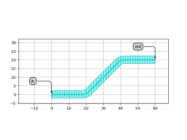
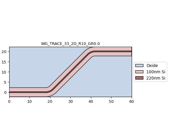
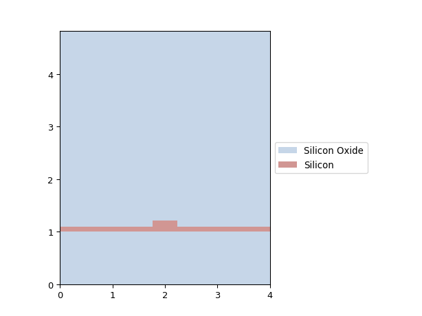
Example
Based on the waveguide template, we can define a waveguide following a given shape, plot its layout and visualize its virtual fabrication (top-down and cross-section). We can also plot the power and phase transmission as a function of wavelength.
"""Plot layout, cross-section and transmission of a silicon wire waveguide."""
import si_fab.all as pdk
import ipkiss3.all as i3
import numpy as np
import matplotlib.pyplot as plt
center_env = i3.Environment(wavelength=1.55)
# Waveguide template: it contains all the cross-sectional information.
wg_tmpl = pdk.SiWireWaveguideTemplate()
wg_tmpl.Layout(core_width=0.47)
wg_tmpl_cm = wg_tmpl.CircuitModel()
print(f"neff @ 1.55: {wg_tmpl_cm.get_n_eff(center_env)}")
print(f"ng @ 1.55: {wg_tmpl_cm.get_n_g(center_env)}")
print(f"loss @ 1.55: {wg_tmpl_cm.get_loss_dB_m(center_env)}")
# Waveguide layout and virtual fabrication
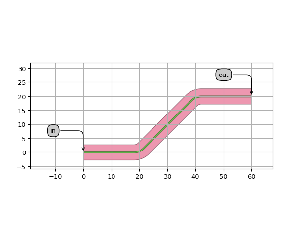
wg = i3.RoundedWaveguide(trace_template=wg_tmpl)
wg_lo = wg.Layout(shape=[(0.0, 0.0), (20.0, 0.0), (40.0, 20.0), (60.0, 20.0)])
wg_lo.visualize(annotate=True)
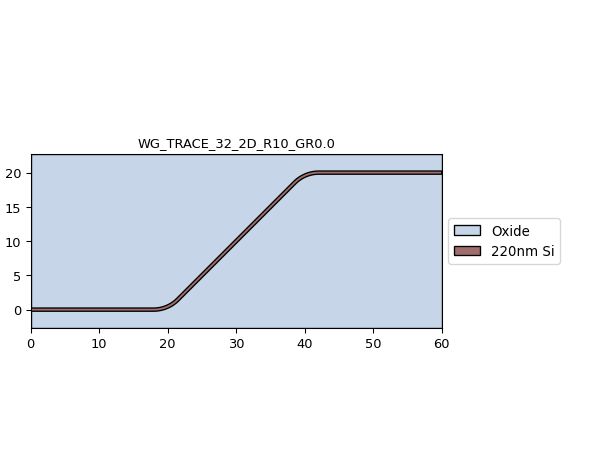
wg_lo.visualize_2d(process_flow=i3.TECH.VFABRICATION.PROCESS_FLOW_FEOL)
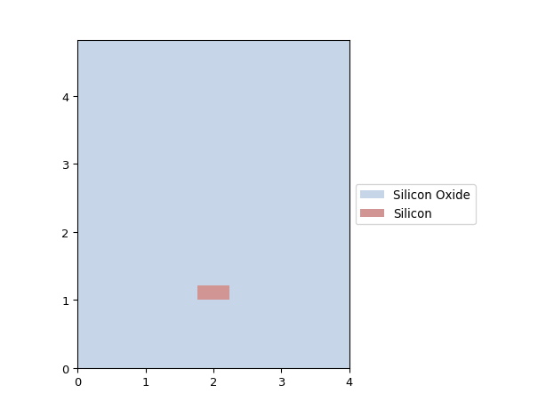
xs = wg_lo.cross_section(cross_section_path=i3.Shape([(1.0, 2.0), (1.0, -2.0)]))
xs.visualize()
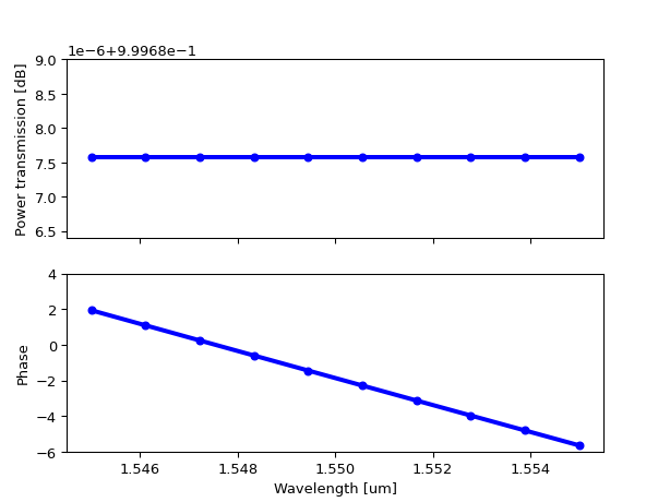
# Plot the power and phase transmission as a function of wavelength
wavelengths = np.linspace(1.545, 1.555, 10)
wg_cm = wg.CircuitModel()
wg_S = wg_cm.get_smatrix(wavelengths)
transmission = wg_S["out", "in"]
fig, (ax1, ax2) = plt.subplots(2, 1, sharex=True)
ax1.plot(wavelengths, np.abs(transmission) ** 2, "bo-", markersize=5, linewidth=3)
ax1.ticklabel_format(axis="y", style="sci", scilimits=(-2, 2))
ax1.set_ylim(0.4 * 1e-6 + 9.99686e-1, 3.0 * 1e-6 + 9.99686e-1)
ax1.set_ylabel("Power transmission [dB]")
ax2.plot(wavelengths, np.unwrap(np.angle(transmission)), "bo-", markersize=5, linewidth=3)
ax2.set_ylim(-6, 4)
ax2.set_xlabel("Wavelength [um]")
ax2.set_ylabel("Phase")
plt.show()
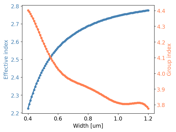
Dispersion diagram
The effective and group indices of the waveguide as a function of width can be visualized as follows:
"""Plot waveguide template dispersion diagram: neff/ng as function of width."""

import si_fab.all as pdk
import ipkiss3.all as i3
import numpy as np
import matplotlib.pyplot as plt

center_env = i3.Environment(wavelength=1.55)
widths = np.linspace(0.4, 1.2, 100)
neffs = []
ngs = []

for w in widths:
    tmpl = pdk.SiWireWaveguideTemplate()
    tmpl.Layout(core_width=w)
    tmpl_cm = tmpl.CircuitModel()
    neffs.append(tmpl_cm.get_n_eff(center_env))
    ngs.append(tmpl_cm.get_n_g(center_env))

fig, ax1 = plt.subplots()

ax1.plot(widths, neffs, "o-", markersize=5, linewidth=3, color="steelblue")
ax1.set_xlabel("Width [um]", fontsize=14)
ax1.set_ylabel("Effective index", color="steelblue", fontsize=14)
ax1.tick_params(axis="y", labelcolor="steelblue", labelsize=14)
ax1.tick_params(axis="x", labelcolor="black", labelsize=14)

ax2 = ax1.twinx()
ax2.plot(widths, ngs, "o-", markersize=5, linewidth=3, color="coral")
ax2.set_ylabel("Group index", color="coral", fontsize=14)
ax2.tick_params(axis="y", labelcolor="coral", labelsize=14)

fig.tight_layout()
plt.show()
Rib waveguide templates
SiFab contains silicon rib waveguide templates, which have a rectangular cross-section shallow etched through the silicon layer.
The waveguide template
SiRibWaveguideTemplateis parametric in width and wavelength. It contains all the cross-sectional information about the wire waveguide: how to draw the layout and the simulation model parameters, such as the effective and group indices.Several fixed-width templates are defined:
RWG450,RWG850.
Example
Based on the waveguide template, we can define a waveguide following a given shape, plot its layout and visualize its virtual fabrication (top-down and cross-section). We can also plot the power and phase transmission as a function of wavelength.
"""Plot layout, cross-section and transmission of a silicon rib waveguide."""
import si_fab.all as pdk
import ipkiss3.all as i3
import numpy as np
import matplotlib.pyplot as plt
center_env = i3.Environment(wavelength=1.55)
# Waveguide template: it contains all the cross-sectional information.
wg_tmpl = pdk.SiRibWaveguideTemplate()
wg_tmpl.Layout(core_width=0.47)
wg_tmpl_cm = wg_tmpl.CircuitModel()
print(f"neff @ 1.55: {wg_tmpl_cm.get_n_eff(center_env)}")
print(f"ng @ 1.55: {wg_tmpl_cm.get_n_g(center_env)}")
print(f"loss @ 1.55: {wg_tmpl_cm.get_loss_dB_m(center_env)}")
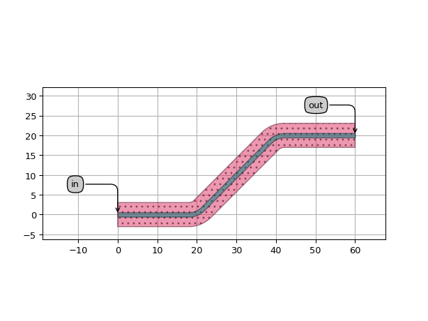
# Waveguide layout and virtual fabrication
wg = i3.RoundedWaveguide(trace_template=wg_tmpl)
wg_lo = wg.Layout(shape=[(0.0, 0.0), (20.0, 0.0), (40.0, 20.0), (60.0, 20.0)])
wg_lo.visualize(annotate=True)
wg_lo.visualize_2d(process_flow=i3.TECH.VFABRICATION.PROCESS_FLOW_FEOL)
xs = wg_lo.cross_section(cross_section_path=i3.Shape([(1.0, 2.0), (1.0, -2.0)]))
xs.visualize()
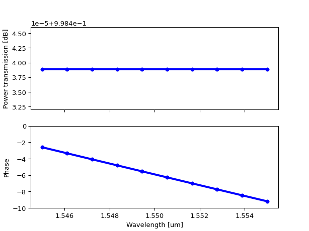
# Plot the power and phase transmission as a function of wavelength
wavelengths = np.linspace(1.545, 1.555, 10)
wg_cm = wg.CircuitModel()
wg_S = wg_cm.get_smatrix(wavelengths)
transmission = wg_S["out", "in"]
fig, (ax1, ax2) = plt.subplots(2, 1, sharex=True)
ax1.plot(wavelengths, np.abs(transmission) ** 2, "bo-", markersize=5, linewidth=3)
ax1.ticklabel_format(axis="y", style="sci", scilimits=(-2, 2))
ax1.set_ylim(0.2 * 1e-5 + 9.9843e-1, 1.6 * 1e-5 + 9.9843e-1)
ax1.set_ylabel("Power transmission [dB]")
ax2.plot(wavelengths, np.unwrap(np.angle(transmission)), "bo-", markersize=5, linewidth=3)
ax2.set_ylim(-10, 0)
ax2.set_xlabel("Wavelength [um]")
ax2.set_ylabel("Phase")
plt.show()
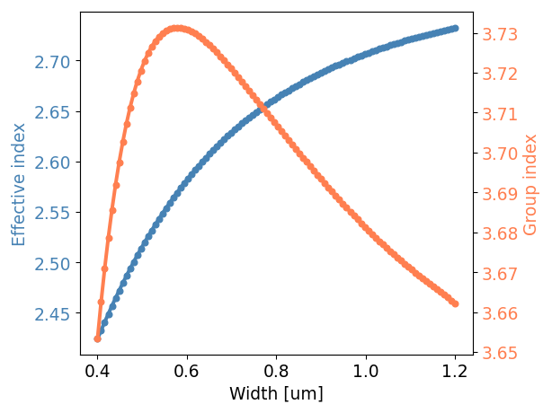
Dispersion diagram
The effective and group indices of the waveguide as a function of width can be visualized as follows:
"""Plot waveguide template dispersion diagram: neff/ng as function of width."""

import si_fab.all as pdk
import ipkiss3.all as i3
import numpy as np
import matplotlib.pyplot as plt

center_env = i3.Environment(wavelength=1.55)
widths = np.linspace(0.4, 1.2, 100)
neffs = []
ngs = []

for w in widths:
    tmpl = pdk.SiRibWaveguideTemplate()
    tmpl.Layout(core_width=w)
    tmpl_cm = tmpl.CircuitModel()
    neffs.append(tmpl_cm.get_n_eff(center_env))
    ngs.append(tmpl_cm.get_n_g(center_env))

fig, ax1 = plt.subplots()

ax1.plot(widths, neffs, "o-", markersize=5, linewidth=3, color="steelblue")
ax1.set_xlabel("Width [um]", fontsize=14)
ax1.set_ylabel("Effective index", color="steelblue", fontsize=14)
ax1.tick_params(axis="y", labelcolor="steelblue", labelsize=14)
ax1.tick_params(axis="x", labelcolor="black", labelsize=14)

ax2 = ax1.twinx()
ax2.plot(widths, ngs, "o-", markersize=5, linewidth=3, color="coral")
ax2.set_ylabel("Group index", color="coral", fontsize=14)
ax2.tick_params(axis="y", labelcolor="coral", labelsize=14)

fig.tight_layout()
plt.show()
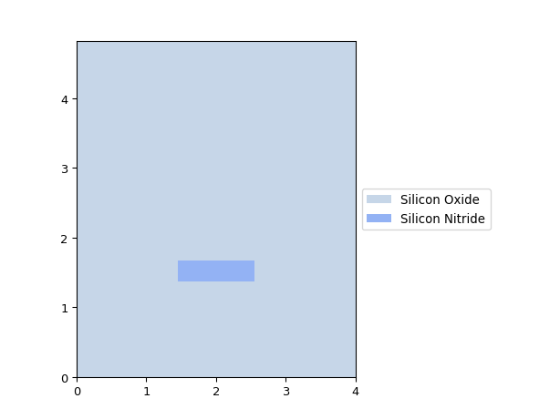
SiN wire waveguide templates
SiFab contains silicon nitride wire waveguide templates, which have a rectangular cross-section shallow etched through the silicon layer.
The waveguide template
SiNWireWaveguideTemplateis parametric in width and wavelength. It contains all the cross-sectional information about the wire waveguide: how to draw the layout and the simulation model parameters, such as the effective and group indices.Several fixed-width templates are defined:
NWG900,NWG1000,NWG1200.
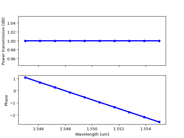
Example
Based on the waveguide template, we can define a waveguide following a given shape, plot its layout and visualize its virtual fabrication (top-down and cross-section). We can also plot the power and phase transmission as a function of wavelength.
"""
Plot layout, cross-section and transmission of a silicon nitride wire waveguide.
"""
import si_fab.all as pdk
import ipkiss3.all as i3
import numpy as np
import matplotlib.pyplot as plt
center_env = i3.Environment(wavelength=1.55)
# Waveguide template: it contains all the cross-sectional information.
wg_tmpl = pdk.SiNWireWaveguideTemplate()
wg_tmpl.Layout(core_width=1.1)
wg_tmpl_cm = wg_tmpl.CircuitModel()
print(f"neff @ 1.55: {wg_tmpl_cm.get_n_eff(center_env)}")
print(f"ng @ 1.55: {wg_tmpl_cm.get_n_g(center_env)}")
print(f"loss @ 1.55: {wg_tmpl_cm.get_loss_dB_m(center_env)}")
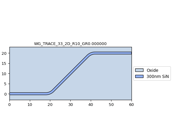
# Waveguide layout and virtual fabrication
wg = i3.RoundedWaveguide(trace_template=wg_tmpl)
wg_lo = wg.Layout(shape=[(0.0, 0.0), (20.0, 0.0), (40.0, 20.0), (60.0, 20.0)])
wg_lo.visualize(annotate=True)
wg_lo.visualize_2d(process_flow=i3.TECH.VFABRICATION.PROCESS_FLOW_FEOL)
xs = wg_lo.cross_section(cross_section_path=i3.Shape([(1.0, 2.0), (1.0, -2.0)]))
xs.visualize()
# Plot the power and phase transmission as a function of wavelength
wavelengths = np.linspace(1.545, 1.555, 10)
wg_cm = wg.CircuitModel()
wg_S = wg_cm.get_smatrix(wavelengths)
transmission = wg_S["out", "in"]
fig, (ax1, ax2) = plt.subplots(2, 1, sharex=True)
ax1.plot(wavelengths, np.abs(transmission) ** 2, "bo-", markersize=5, linewidth=3)
ax1.ticklabel_format(axis="y", style="sci", scilimits=(-2, 2))
ax1.set_ylabel("Power transmission [dB]")
ax2.plot(wavelengths, np.unwrap(np.angle(transmission)), "bo-", markersize=5, linewidth=3)
ax2.set_xlabel("Wavelength [um]")
ax2.set_ylabel("Phase")
plt.show()
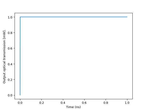
Time domain diagram
Transmission of the waveguide as a function of the time can be visualized as follows:
"""
Plot layout and transmission of a silicon nitride wire waveguide.
"""

import si_fab.all as pdk
import ipkiss3.all as i3
import numpy as np
import matplotlib.pyplot as plt

wg_tmpl = pdk.SiNWireWaveguideTemplate()
wg_tmpl.Layout(core_width=1.1)

# Waveguide layout
wg = i3.RoundedWaveguide(trace_template=wg_tmpl)
wg_lo = wg.Layout(shape=[(0.0, 0.0), (20.0, 0.0), (40.0, 20.0), (60.0, 20.0)])


def opt_signal(t):
    # The optical input signal is a CW laser. It's modulated around 'center_frequency', a parameter that's passed on
    # to get_time_response. We return the amplitude + phase here.
    # For example, 1 mW is represented by sqrt(1e-3).
    return np.sqrt(1.0 * 1e-3)


testbench = i3.ConnectComponents(
    child_cells={
        "wg": wg,
        "input_optical": i3.FunctionExcitation(
            port_domain=i3.OpticalDomain,
            excitation_function=opt_signal,
        ),
        "output_optical": i3.Probe(port_domain=i3.OpticalDomain),
    },
    links=[
        ("input_optical:out", "wg:in"),
        ("output_optical:in", "wg:out"),
    ],
)

cm = testbench.CircuitModel()

t0 = 0
t1 = 1e-9
dt = 1e-12

response = cm.get_time_response(t0=t0, dt=dt, t1=t1, center_wavelength=1.55)

plt.plot(response.timesteps * 1e9, np.abs(response["output_optical"]) ** 2 * 1e3)
plt.xlabel("Time (ns)")
plt.ylabel("Output optical transmission [mW].")
plt.show()
Note
The above simulation results are artificial results as they’re based on fictional technology and components. These only serve demonstration purposes.