
Luceda ADK for PHIX
The Assembly Design Kit (ADK) for PHIX is a design kit for packaging photonic ICs with the PHIX packaging foundry
Contents
PDK Documentation
This document explains how to use the Luceda Assembly Design Kit (ADK) for the PHIX Characterization Package (version 1.3.1.luceda1).
The ADK can be used from IPKISS, providing the following functionality:
definition and layout of circuits within PHIX’s Characterization Package, which is entirely available within IPKISS
This document explains how to get started with the ADK, lists the cells that are available and documents the technology for custom design.
Document information
License
The use of this ADK is subject to the “PHIX User Non-Disclosure Agreement”.
Usage and responsibility
The use of this ADK is restricted to the design of photonic integrated circuits in the PHIX platform, fabricated by PHIX (Foundry).
All relevant documentation about the PHIX platform, including process description and design rules, can be found in the PHIX Design Manual as provided by the Foundry. The user is advised to carefully read the PHIX Design Manual.
It is the user’s responsibility to verify that the design, made on the basis of this Assembly Design Kit, meets the Foundry’s design rules.
In case of doubt, the user should consider the Foundry’s design rule manual as the correct reference (as validated by the Foundry).
Under no circumstances does LUCEDA represent or warrant that operation of the photonic integrated circuits by the Foundry, designed on the basis of this Assembly Design Kit, will be error-free or will accord to the user specifications, and hereby disclaims all liability on account thereof.
Changelog
This changelog shows the changes in the Luceda ADK for the PHIX Characterization Package.
1.3.1.luceda1
Fixed import to work with new Luceda IPKISS tech defining functionalities
1.3.1
Added RFCharacterizationPackage
Updated CharacterizationPackage parameters and markers
Added the possibility to give different number of pads and optical couplers on each side
1.1
Fixed marker_layer property definition
1.0
PackageTemplate renamed to CharacterizationPackage
Fixed TECH.GDSII.LAYERTABLE_PDK to contain only PDK layers
Renamed CharacterizationPackage ports using cardinal directions
Added coupler and pad childcell to CharacterizationPackage
Added marker_layer to generate alignment markers also with a PDK layer
0.1 Initial release
Technology setup
Parametric characterization package template
Getting Started
This section explains how to load the Luceda ADK for the PHIX Characterization Package and basics of how to use it.
If you are unfamiliar with IPKISS, please have a look at the IPKISS documentation and samples. The documentation and samples are available from the IPKISS Control Center.
The latest IPKISS documentation is also available online at http://academy.lucedaphotonics.com.
Extracting the ADK
The ADK is distributed as a zip file, which you can extract with the unzip utility of your choice (unzip, WinZip, 7-zip, …).
For the purpose of this manual, we assume you have unzipped “phix.x.x_buildnr.zip” as C:\designs\pdks\phix.
You can inspect the directory structure of the ADK:
docs/: Contains this file
docs/examples/: Example IPKISS python scripts
ipkiss/: IPKISS technology, cells and functions (Python)
techfiles/: Tech files (layers, display) for various tools
techfiles/klayout/: Layer settings for KLayout GDSII visualization
Using the ADK with IPKISS
Setting up the editor environment
You can follow the instructions given in our documentation https://academy.lucedaphotonics.com/tutorials/environment_setup/create_project_pdk.html.
Examples
The ADK comes bundled with a series of examples for use in IPKISS, in the <path_to_pdk>\docs\examples. These are executable Python files. The examples are a good starting point to learn how to design with this ADK. Below is a summary of the shipped examples:
Example name |
Description |
|---|---|
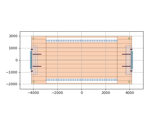
example_ec.py |
Visualize a RF packaging template using Edge couplers |
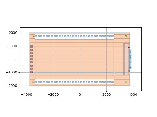
example_gc.py |
Visualize a packaging template using Grating couplers |
Technology settings
The ADK contains layer definitions. Note that, for the best usage, a IPKISS technology (Luceda PDK) must be loaded before importing the ADK.
Layers
The following table gives an overview of the available layers and how they are named in Ipkiss. See the PHIX design rules manual for further information about the layers defined by PHIX.
IPKISS Layer (TECH.PPLAYER.) |
Description |
GDS Number |
|---|---|---|
PIC_DIM |
PIC dimensions |
2015, 10 |
PIC_RULERS |
PIC rulers |
2015, 11 |
PIC_MARKS |
PIC marks |
2015, 12 |
EC_LOC |
EC-locations |
2015, 21 |
GC_LOC |
GC-locations |
2015, 25 |
EC_BP |
EC-Bondpad |
2015, 58 |
GC_BP |
GC-Bondpad |
2015, 59 |
EC_EPOXY |
EC-epoxy area |
2015, 71 |
GC_EPOXY |
GC-epoxy area |
2015, 75 |
EC_KEEP_OUT |
EC-BP keep-out |
2015, 81 |
GC_KEEP_OUT |
GC-BP keep-out |
2015, 85 |
WIRE_BOND |
Wire bonds |
2015, 100 |
ADK Packaging Template
The library contains two packaging template classes.
CharacterizationPackage
- class phix.all.CharacterizationPackage(*args, **kwargs)
PHIX Characterization Package Template.
Ports are named according to the side they’re on (north, south, east or west) and numbered from west to east and south to north starting from 1.
For example, “east_1” is most south-east coupler marker if no coupler provided. Otherwise, “east_in_1” is most south-east coupler waveguide port and “east_out_1” is fiber coupling port. “north_1” is the most north-west pad marker if no pad provided. Otherwise, “north_{pad_port}_1” is the {pad_port} of the most west north pad.
- Parameters:
- pad_to_edge: float and number > 0 and [100,500]
Pad to PIC edge (min 100 if Fab-diced and 300 for PHIX-dicing) [um]
- pad_dim: float and number > 0 and [90,150]
Pad side size 120 (+/-30) [um]
- pad_pitch: float and number > 0 and [150,350]
Pad pitch 200 (+/-50) [um]
- pad_number:
Number of pads per side, range between 0 and 60. Or a tuple of the number of couplers on north and south. A single number will result in north and south having the same number.
- couplers_pitch: float and number > 0 and List with value restriction, allowed values: (127.0, 250.0)
Coupler pitch (up to 12ch for 250um possible)
- couplers_number:
Number of couplers (max 32 for 127um pitch and 12 for 250um pitch), or tuple of the number of couplers on east and number of couplers on west. A single number will result in west and east having the same number.
- couplers_type:
Grating couplers (True) or Edge couplers (False) markers
- location_ruler_y: float and number > 0
Y spacing from 1st and last optical coupler [um]
- location_ruler_x: float and int, float, integer, floating and number >= 0
X location: match waveguide-end with 0 [um]
- pic_length: float and number > 0 and [4000,20000]
PIC length [um]
- pic_width: float and number > 0 and [4000,20000]
PIC width [um]
- marker_layer: ( __Layer__ ), *None allowed*
Layer of the markers used for alignment (metal layer recommended for higher contrast).
- pad: ( PCell ), *None allowed*
Bondpad used at every marker
- coupler: ( PCell ), *None allowed*
Coupler used at every marker
RFCharacterizationPackage
- class phix.all.RFCharacterizationPackage(*args, **kwargs)
PHIX RF Characterization Package Template.
Ports are named according to the side they’re on (north, south, east or west) and numbered from west to east and south to north starting from 1.
For example, “east_1” is most south-east coupler marker if no coupler provided. Otherwise, “east_in_1” is most south-east coupler waveguide port and “east_out_1” is fiber coupling port. “north_1” is the most north-west pad marker if no pad provided. Otherwise, “north_{pad_port}_1” is the {pad_port} of the most west north pad.
- Parameters:
- rfpad_to_edge: float and number > 0 and [30,100]
rf Pad to PIC edge [um]
- rfpad_size: float and number > 0
RF pad dimension (140 or 100 recommended) [um]
- rfpad_pitch: float and number > 0
RF signal pitch (720 or 600 recommended) [um]
- rfpad_number: int and number >= 0 and [0,16]
Number of RF pads
- pad_to_edge: float and number > 0 and [100,500]
Pad to PIC edge (min 100 if Fab-diced and 300 for PHIX-dicing) [um]
- pad_dim: float and number > 0 and [90,150]
Pad side size 120 (+/-30) [um]
- pad_pitch: float and number > 0 and [150,350]
Pad pitch 200 (+/-50) [um]
- pad_number:
Number of pads per side, range between 0 and 60. Or a tuple of the number of couplers on north and south. A single number will result in north and south having the same number.
- couplers_pitch: float and number > 0 and List with value restriction, allowed values: (127.0, 250.0)
Coupler pitch (up to 12ch for 250um possible)
- couplers_number: int and number >= 0 and [0,60]
Number of couplers (max 32 for 127um pitch and 12 for 250um pitch) on east.
- location_ruler_y: float and number > 0
Y spacing from 1st and last optical coupler [um]
- location_ruler_x: float and int, float, integer, floating and number >= 0
X location: match waveguide-end with 0 [um]
- pic_length: float and number > 0 and [4000,20000]
PIC length [um]
- pic_width: float and number > 0 and [4000,20000]
PIC width [um]
- marker_layer: ( __Layer__ ), *None allowed*
Layer of the markers used for alignment (metal layer recommended for higher contrast).
- pad: ( PCell ), *None allowed*
Bondpad used at every marker
- coupler: ( PCell ), *None allowed*
Coupler used at every marker
PHIX Characterization Package Template. |
|
PHIX RF Characterization Package Template. |