
Luceda PDK for CORNERSTONE SOI
The Luceda PDK for CORNERSTONE SOI allows to design and tape out to CORNERSTONE SOI process.
Regarding CORNERSTONE SOI process, additional information can be found here.
Contents
PDK Documentation

This document explains how to use the Luceda Process Design Kit (PDK) for CORNERSTONE (version 2.6.luceda1).
The PDK can be used from Luceda IPKISS, providing the following functionality:
definition and layout of circuits using CORNERSTONE’s predefined library of cells (building blocks), which is entirely available within IPKISS,
waveguide routing using the waveguide types defined by CORNERSTONE, or custom defined waveguides following CORNERSTONE design rules,
definition of custom devices using CORNERSTONE layers and design rules,
simulation of custom devices using IPKISS’ built-in solvers and interfaces to 3rd party tools such as Dassault Systems CST Studio Suite and Lumerical FDTD Solutions,
circuit editing from Siemens L-Edit using Luceda Link for Siemens EDA.
This document explains how to get started with the PDK, lists the cells that are available and documents the technology for custom design.
Changelog
This changelog shows the changes in the Luceda PDK for CORNERSTONE.
2.6.luceda1
Updated the PDK to work with Luceda 3.10 and 3.11 software. Don’t use the PDK with Luceda 3.9 anymore.
2.6
Updated SOI340nm_1310nm_TE_STRIP_2X2_MMI
Added an .iclib file (library file recognized by IPKISS Canvas) with symbol drawings
2.5.luceda1
Updated for IPKISS 3.9. The PDK runs on Python3 as well as Python2 IPKISS 3.9 is required to run the PDK
2.5
Updated for IPKISS 3.7
2.4
Updated SOI220nm_1550nm_TE_STRIP_2X1_MMI, SOI220nm_1550nm_TE_RIB_2X1_MMI
Updated SOI340nm_1310nm_TE_STRIP_2X2_MMI, SOI340nm_1310nm_TE_RIB_2X2_MMI
2.3
Added: SOI220nm_1550nm_TE_RIB_Grating_Coupler, SOI220nm_1550nm_TE_STRIP_2X1_MMI, SOI220nm_1550nm_TE_STRIP_2x2_MMI, SOI220nm_1550nm_TE_STRIP_2x1_Ysplitter, SOI220nm_1550nm_TE_STRIP_Grating_Coupler, SOI220nm_1550nm_TM_STRIP_Grating_Coupler, SOI220nm_1310nm_TE_RIB_Grating_Coupler, SOI220nm_1310nm_TE_STRIP_2X1_MMI, SOI220nm_1310nm_TE_STRIP_2x2_MMI, SOI220nm_1310nm_TE_STRIP_2x1_Ysplitter, SOI220nm_1310nm_TE_STRIP_Grating_Coupler, SOI220nm_1310nm_TM_STRIP_Grating_Coupler, SOI340nm_1550nm_TE_STRIP_Grating_Coupler, SOI340nm_1310nm_TE_STRIP_Grating_Coupler, SOI340nm_1550nm_TE_RIB_STRIP_Apodised_Grating_Coupler, SOI340nm_1550nm_TE_RIB_RIB_Apodised_Grating_Coupler, SOI500nm_1550nm_TE_RIB_2X2_MMI, SOI500nm_1550nm_TE_RIB_Grating_Coupler and SOI500nm_1550nm_TM_RIB_Grating_Coupler
Updated SOI220nm_1550nm_TE_RIB_2X1_MMI, SOI220nm_1310nm_TE_RIB_2X1_MMI, SOI220nm_1310nm_TE_RIB_2x2_MMI, SOI220nm_1310nm_TE_RIB_GC, SOI340nm_1310nm_TE_RIB_GC, SOI340nm_1310nm_TE_STRIP_GC and SOI500nm_1550nm_TE_RIB_2X1_MMI
Updated SOI 500nm vfab
Renamed SOI340nm_1550nm_TE_RIB_STRIP_Apodised_Grating_Coupler to SOI340nm_1550nm_TE_RIB_STRIP_Apodised_Grating_Coupler
2.2.luceda1
Updated this PDK to be compatible with IPKISS 3.4
Renamed OA folder to openaccess
2.2
Important: Only update of 340nm (later 220 and 500)
Updated 340nm components
Added 340nm components
Added Ebeam and Blocking layers
2.1
global: add RIB_AllPass_Ring, RIB_AddDrop_Ring, STRIP_AllPass_Ring and STRIP_AddDrop_Ring
rename SOI220nm_1550nm_TE_RIB_Grating_Coupler_RIBTapered to …._Coupler_RibTapered
2.0
Important: No backward compatibilty!
Updates in view of CORNERSTONE MPW call 11
global: renamed all the components to make their application case (wavelength and polarization) more clear
global: 1x2 MMI replaced by 2x1 MMI
global: remove parametric crossings
220nm SOI: change the MZIs (1.5um modulator length instead of 1.8um)
220nm SOI: fix the predefined crossings
340nm SOI: change the components from Strip to Rib
1.3.0
Updates in view of CORNERSTONE MPW call 10
global: change the way to select the technology (see
technology)global: add label layer (GDS 100)
global: add parametric crossings and rib modulator
220nm SOI technology: update some dimensions
200nm SOI devices added: fixed crossings and Mach-Zehnder modulators
1.2.0
Updates in view of CORNERSTONE MPW call 9
500nm SOI technology variant added + example scripts
500nm SOI devices added: grating coupler and MMI
PHC layer added for photonic crystal devices
1.1.0
Updates in view of CORNERSTONE MPW call 7
1.0.1
Fix: the predefined grating couplers now have 60 grating periods
1.0.0
Initial Luceda PDK for CORNERSTONE release:
Technology settings, drawing layers, GDSII, IPKISS Link for Siemens EDA compatibility, waveguides, MMI and grating coupler building blocks, virtual fabrication for passives
The technology settings (virtual fabrication) has both 220nm and 340nm SOI flavours. The device library is 220nm SOI only at this point
Introduction
Process Design Kit (PDK) based design concept
If you already know about Process Design Kits (PDKs) in general, please skip to the section Getting started.
A PDK helps to bridge the gap between the fab or foundry offering IC technology and the designer who creates an IC design in that technology, as shown by Figure 1. In order to create a design, the designer needs to have the library cells created by the fab available, as well as technology details required for custom design of components. A PDK is implemented for a specific set of software tools.

Fig. 1 Concept of a Process Design Kit (PDK)
Luceda develops such a PDK so that it can be used by the Luceda tools (Link for Siemens EDA or IPKISS).
Luceda PDK has several components:
Technology settings that allow for custom design:
Layers to draw with, in accordance with the foundry’s definitions.
Design rules, which provide dimensional constraints for the design to be manufacturable.
A design rule checking (DRC) deck, checking that the designer’s mask layout adheres to the foundry’s design rules.
A technology description that allows to generate 2D and 3D models that can be sent to physical simulation tools such as for FDTD or mode propagation.
Routing settings for optical waveguides and electrical wiring
The fab’s cell library, providing validated building blocks to the designer:
Layout models that allow to place and connect the cells in the layout. These can be ‘black-box’: the detailed layout may not be visible, only the optical and electrical I/O and the bounding box.
Simulation models that allow for simulation and functional verification of a circuit based on these cells.
Parametric cells for typical complex cells or repetitive tasks that a designer would like to do
Examples and (this) manual to get started
The combination of Luceda’s design software and the Luceda PDK for CORNERSTONE is what enables the designer to create a design specific for the CORNERSTONE technology.
Note
In this text, the words cell, component and building block are used interchangeably. In the context of a PDK, a cell, building block or component usually delivers a specific unit function, such as a fiber coupler, splitter or phase modulator. There could also be more complex cells in the PDK library though. In the context of the user design, cell could mean any design or hierarchical part thereof.
Use case: PDK cell library based design
The Luceda PDK for CORNERSTONE provides a library with a number of predefined cells for the C band (1550nm) and O band (1310nm). With this library available from IPKISS, the designer can create a circuit directly in code (IPKISS) or from the L-Edit GUI using drag-and-drop of devices from the library (IPKISS Link for Siemens EDA). After placing the PDK cells, optical waveguides can be drawn in a manual or semi-automated fashion. In addition, the PDK provides the necessary settings to use picazzo, Luceda’s pcell template library with functions like ring resonators, MMIs, modulators, Mach-Zehnder interferometers, fanouts, and many more.
This approach allows for fast prototyping of designs using the CORNERSTONE technology.
Use case: Custom cell design
In a lot of cases, the user will want to design custom components and include them in the design. IPKISS provides several functions for that purpose:
Parametric cells can be defined fully in Python script, with their parameters (properties in IPKISS), layout and simulation model.
Basic building blocks can be virtually fabricated and sent to electromagnetic simulation tools such as FDTD and EME. IPKISS has a built-in mode solver CAMFR and provides interfaces to CST Studio suite and other 3rd party tools.
More complex subcircuits defined in IPKISS can be simulated using the built-in compact model solver Caphe. The designer can provide models for the basic building blocks, or generate them from simulation or measurement data.
The designer can maintain the resulting parametric cells in a library and use them from the IPKISS Link for Siemens EDA environment or in an IPKISS python code design.
Use case: Using internal and 3rd party libraries
In a larger design team or in the case of consecutive design projects, a designer or a design team will typically build up their own library of subcircuits that perform specific reusable functions. Using Luceda’s software, the designer or design team can create such proprietary libraries that work together with the Luceda PDK for CORNERSTONE. These re-usable libraries can then be shared within the team, outside of the company or used in consecutive projects.
The designer can in this way embed and sustain design knowledge in a library, and base a new design both on the PDK as well as these internal libraries.
One step further, a designer can also acquire 3rd party libraries and use them in a design project in the same way.

Fig. 2 Designing with reuseable design libraries and a PDK.
Getting Started
This section explains how to load the PDK in IPKISS and basics of how to use it.
If you are unfamiliar with Luceda IPKISS, please have a look at the IPKISS documentation and samples. The documentation and samples are available from the IPKISS Control Center.
The latest IPKISS documentation is also available online at http://docs.lucedaphotonics.com/index.html.
Extracting the PDK
The PDK is distributed as a zip file, which you can extract with the unzip utility of your choice (unzip, WinZip, 7-zip, …).
For the purpose of this manual, we assume you have unzipped “cornerstone-2.6.luceda1.zip” as C:\temp\cornerstone.
You can inspect the directory structure of the PDK:
data/: Contains GDS files of some fixed cells
docs/: Contains this file
docs/examples/scripts: Example IPKISS python scripts
docs/examples/lib.defs: Example of IPKISS Link for Siemens EDA design project
ipkiss/: IPKISS technology, pcells, models and functions (Python)
ipkiss/conerstone/cornerstone.iclib: Symbol library for the PDK (IPKISS Canvas)
openaccess/: Design libraries
openaccess/cornerstone/: OpenAccess database for the PDK (L-Edit)
techfiles/: Tech files (layers, display) for various tools
techfiles/klayout/: Layer settings for KLayout GDSII visualization
Using the PDK with IPKISS Link for Siemens EDA
You can follow the instructions given in our documentation https://docs.lucedaphotonics.com/links/ipkisseda/ledit/tutorial_pdk_based_circuit/.
Using the PDK with IPKISS
Setting up the editor environment
You can follow the instructions given in our documentation https://docs.lucedaphotonics.com/tutorials/environment_setup/create_project_pdk
Examples
The PDK comes bundled with a series of examples for use in IPKISS, in the C:\temp\cornerstone\docs\examples\scripts folder. These are executable Python files. The examples are a good starting point to learn how to design with the Luceda PDK for CORNERSTONE. Below is a summary of the shipped examples:
Example name
Description
example_layers.py
Visualize all the layers that are available in the cornerstone technology
example_waveguides.py
Visualize the waveguides available in the cornerstone technology
example_heater.py
Example of a waveguide with a heater filament
example_mzi.py
Example of MZI circuit exported to IPKISS Canvas
example_design_passive.py
Example of a parameter sweep of ring resonators with automated fiber coupler embedding
example_modulator_vfab.py
Example of a cross section visualization for one of the fixed MZM
example_customcell.py
Create a custom PCell in IPKISS using the CORNERSTONE technology
example_phc_soi220.py
Example of a photonic crystal component using the Luceda picazzo3 library for 220nm platform
example_components_220.py
Shows the PDK components for 220nm platform
example_phc_soi340.py
Example of a photonic crystal component using the Luceda picazzo3 library for 340nm platform
example_components_340.py
Shows the PDK components for 340nm platform
example_phc_soi500.py
Example of a photonic crystal component using the Luceda picazzo3 library for 500nm platform
example_components_500.py
Shows the PDK components for 500nm platform
References
IPKISS documentation: http://docs.lucedaphotonics.com/index.html
Library organization: https://docs.lucedaphotonics.com/links/ipkisseda/libraries/library_organization/
Technology settings
The PDK contains layer definitions and virtual fabrication settings for the 220nm, 340nm and 500nm SOI processes. Refer to the CORNERSTONE design rule manual and MPW call documents for detailed information.
Selecting the target technology
One PDK is used to target all the technologies. At the start of an Ipkiss script, you must import the library corresponding to the technology variant you need.
For example, the 220nm SOI process:
import cornerstone_soi220.all as cornerstone
This sets the virtual fabrication process of the 220nm SOI process and imports only the process specific components and the generic pcells.
Process |
Library |
Specific cells prefix |
|---|---|---|
220nm SOI |
cornerstone_soi220 |
SOI220nm |
340nm SOI |
cornerstone_soi340 |
SOI340nm |
500nm SOI |
cornerstone_soi500 |
SOI500nm |
Layers
The following table gives an overview of the available layers and how they are named in Ipkiss. See the CORNERSTONE design rules manual for further information about the layers defined by CORNERSTONE.
Layer name |
Description |
IPKISS Layer |
GDS Number |
|---|---|---|---|
WG |
Silicon Etch - Waveguides (Light field) |
TECH.PPLAYER.WG |
3/0 |
WG_HOL |
Silicon Etch - Waveguides (Dark field) |
TECH.PPLAYER.WG_HOL |
4/0 |
GRAT |
Silicon Etch - Gratings |
TECH.PPLAYER.GRAT |
6/0 |
SLAB |
Silicon Etch - Rib Protect |
TECH.PPLAYER.SLAB |
5/0 |
P |
Low Dose p-type Implant |
TECH.PPLAYER.P |
7/0 |
N |
Low Dose n-type Implant |
TECH.PPLAYER.N |
8/0 |
PPLUS |
High Dose p-type Implant |
TECH.PPLAYER.PPLUS |
9/0 |
NPLUS |
High Dose n-type Implant |
TECH.PPLAYER.NPLUS |
11/0 |
VIA |
Vias - rounded features corners |
TECH.PPLAYER.VIA |
12/0 |
M1 |
Electrodes - min gap between features = 2µm |
TECH.PPLAYER.M1 |
13/0 |
HT |
Heater Filaments |
TECH.PPLAYER.HT |
39/0 |
PAD |
Heater Contact Pads |
TECH.PPLAYER.PAD |
41/0 |
PHC |
Silicon Etch - Photonic Crystals |
TECH.PPLAYER.PHC |
42/0 |
EBEAM |
E-beam etch layer |
TECH.PPLAYER.EBEAM |
60/0 |
BLOCK |
Protection layer for waveguide etch |
TECH.PPLAYER.BLOCK |
61/0 |
CELL |
Cell Outline |
TECH.PPLAYER.NONE.CELL |
99/0 |
BLEED |
Bleed Area |
TECH.PPLAYER.NONE.BLEED |
98/0 |
LBL |
Label - DRC purpose layer then included in GDS 4 |
TECH.PPLAYER.NONE.LBL |
100/0 |
STRIP_TRACE |
Strip waveguide routing - Luceda non-tapeout layer |
TECH.PPLAYER.STRIP_TRACE |
|
RIB_TRACE |
Rib waveguide routing - Luceda non-tapeout layer |
TECH.PPLAYER.RIB_TRACE |
Components
Which components are available to use from the Luceda PDK for CORNERSTONE?
The Luceda PDK for CORNERSTONE contains a number of predefined components that have been tested by the fab, as well as predefined waveguide templates. In addition, Luceda has provided a number of parametric cells to make life of a designer easier.
Users can use these components and mix them with their own custom designed components to create larger circuits.
How to use Luceda PDK for CORNERSTONE components?
An example of how to instantiate (or place) PDK components in IPKISS, you may refer the sample located at:
<path_to_installed_PDK>\cornerstone\docs\examples\scripts\example_components.py
For 340nm SOI, refer to the example at <path_to_installed_PDK>\cornerstone\examples\scripts\example_components_soi340.py
With IPKISS, you may execute the sample Python code.
If you use IPKISS Link for Siemens EDA, you will be able to use your mouse to drag-and-drop the components in L-Edit.
Waveguide template components
Waveguide trace templates are used to define how the connecting waveguides between the devices should be like. It contains the technology information on the layers and geometrical drawing of a specific type of waveguide, such as wire or rib waveguides.
Using the waveguide trace template, when users define the waveguide type at a device port and the connection line with another device, the waveguide will be generated with the corresponding waveguide type at the port it connects to. There are also devices that are drawn using the waveguide template as a layout parameter. It is useful in this case to change the device design by updating the waveguide template.
Two waveguide templates are predefined in the PDK: StripWaveguideTemplate, for strip waveguides fully etched to the BOX, and RibWaveguideTemplate for rib waveguides with a thin SOI slab remaining. Both have a default width of 400nm for O band and 450nm for C band.
These templates have no models yet.
Luceda picazzo components
Besides the component library provided by the foundry, users are also able to use the component templates from IPKISS’ Picazzo library.
Note
Unlike the Luceda PDK for CORNERSTONE components of which device performance is characterized and guaranteed by the fab, the Picazzo library components are up to the user to ensure compatibility with the design rules and the designed device manufacturability and performance.
The list of Picazzo library components and their documentation can be found in the IPKISS manual: https://docs.lucedaphotonics.com/picazzo/
In the documentation examples, we use the silicon_photonics as the technology library (a demo technology library from IPKISS). Now that we have a real-world PDK, we are able to use it as the technology library for the picazzo design.
Photonic crystals
Picazzo offers a lot of components for drawing photonic crystals: https://docs.lucedaphotonics.com/picazzo/phc/ These however need some customization in order to work with CORNERSTONE: the SOI slab area needs to be explicitly added.
For 220nm SOI, an example is in <path_to_installed_PDK>\docs\examples\scripts\example_phc_soi220.py.
For 340nm SOI, an example is in <path_to_installed_PDK>\docs\examples\scripts\example_phc_soi340.py
For 500nm SOI, an example is in <path_to_installed_PDK>\docs\examples\scripts\example_phc_soi500.py
How to customize a component design?
Users can also choose start a component design from scratch, instead of starting from a CORNERSTONE library component or picazzo library component.
An example is given in <path_to_installed_PDK>\docs\examples\scripts\example_customcell.py.
Component List
These components have no models yet.
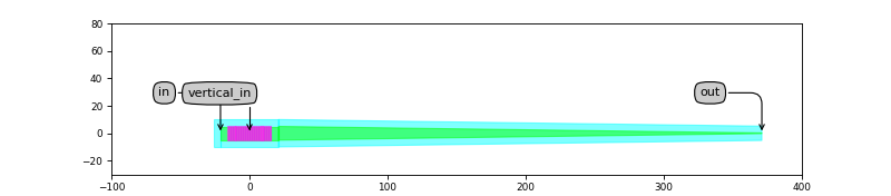
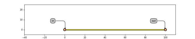
Grating Couplers
RIB_Grating_Coupler
PCell for Grating Coupler in rib waveguide
- Parameters:
- inclination: float
out-of-plane angle of the grating coupler
- name: String that contains only ISO/IEC 8859-1 (extended ASCII py3) or pure ASCII (py2) characters
The unique name of the pcell
- Other Parameters:
- grating: PCell, locked
- socket: PCell, locked
- trace_template: PCell and _TraceTemplate, locked
(Source code, png, hires.png, pdf)
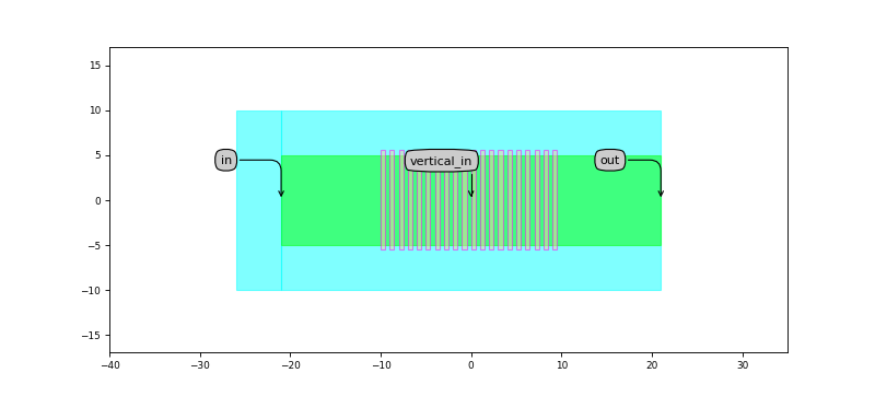
Ports
Name |
Type |
Position |
Angle |
Waveguide Template |
Inclination |
|---|---|---|---|---|---|
in |
Optical |
(-21.0,0.0) |
180.0 |
RibWaveguideTemplate |
0.0 |
out |
Optical |
(21.0,0.0) |
0.0 |
RibWaveguideTemplate |
0.0 |
vertical_in |
Optical |
(0.0,0.0) |
180.0 |
90.0 |
Layout
Parameters
- socket_width: float and number > 0
Width of the grating socket [um]
- line_length: float and number > 0
length of the grating trenches (perpendicular to the socket waveguide)
- line_width: float and number > 0
width of the grating trenches, drawn in the given layer
- n_o_periods: int and number > 0
number of periods of the grating
- origin: Coord2
local origin of the grating (first trench)
- period: float and number > 0
period of the grating
- socket_length: float and number > 0
length of the straight waveguide socket
STRIP_Grating_Coupler
PCell for Grating Coupler in strip waveguide
- Parameters:
- inclination: float
out-of-plane angle of the grating coupler
- name: String that contains only ISO/IEC 8859-1 (extended ASCII py3) or pure ASCII (py2) characters
The unique name of the pcell
- Other Parameters:
- grating: PCell, locked
- socket: PCell, locked
- trace_template: PCell and _TraceTemplate, locked
(Source code, png, hires.png, pdf)
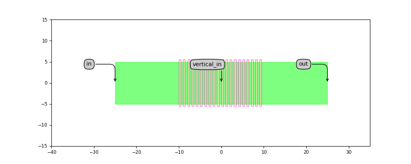
Ports
Name |
Type |
Position |
Angle |
Waveguide Template |
Inclination |
|---|---|---|---|---|---|
in |
Optical |
(-25.0,0.0) |
180.0 |
StripWaveguideTemplate |
0.0 |
out |
Optical |
(25.0,0.0) |
0.0 |
StripWaveguideTemplate |
0.0 |
vertical_in |
Optical |
(0.0,0.0) |
180.0 |
90.0 |
Layout
Parameters
socket_width: float and number > 0 line_length: float and number > 0
length of the grating trenches (perpendicular to the socket waveguide)
- line_width: float and number > 0
width of the grating trenches, drawn in the given layer
- n_o_periods: int and number > 0
number of periods of the grating
- origin: Coord2
local origin of the grating (first trench)
- period: float and number > 0
period of the grating
- socket_length: float and number > 0
length of the straight waveguide socket
220 nm SOI cells
SOI220nm_1550nm_TE_RIB_Grating_Coupler
TE C-band rib grating coupler.
(Source code, png, hires.png, pdf)
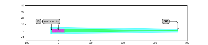
Ports
Name |
Type |
Position |
Angle |
Waveguide Template |
Inclination |
|---|---|---|---|---|---|
out |
Optical |
(371.0,0.0) |
0.0 |
RibWaveguideTemplate |
0.0 |
in |
Optical |
(-21.0,0.0) |
180.0 |
RibWaveguideTemplate |
0.0 |
vertical_in |
Optical |
(0.0,0.0) |
180.0 |
90.0 |
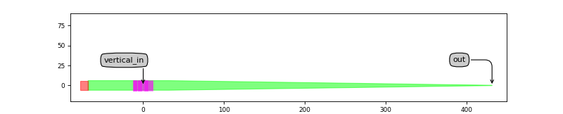
SOI220nm_1550nm_TE_STRIP_Grating_Coupler
TE C-band strip grating coupler.
Ports
Name |
Type |
Position |
Angle |
Waveguide Template |
Inclination |
|---|---|---|---|---|---|
out |
Optical |
(375.0,0.0) |
0.0 |
StripWaveguideTemplate |
0.0 |
in |
Optical |
(-25.0,0.0) |
180.0 |
StripWaveguideTemplate |
0.0 |
vertical_in |
Optical |
(0.0,0.0) |
180.0 |
90.0 |
SOI220nm_1550nm_TM_STRIP_Grating_Coupler
TM C-band strip grating coupler.
Ports
Name |
Type |
Position |
Angle |
Waveguide Template |
Inclination |
|---|---|---|---|---|---|
out |
Optical |
(375.0,0.0) |
0.0 |
StripWaveguideTemplate |
0.0 |
in |
Optical |
(-25.0,0.0) |
180.0 |
StripWaveguideTemplate |
0.0 |
vertical_in |
Optical |
(0.0,0.0) |
180.0 |
90.0 |
SOI220nm_1310nm_TE_RIB_Grating_Coupler
TE O-band rib grating coupler.
Ports
Name |
Type |
Position |
Angle |
Waveguide Template |
Inclination |
|---|---|---|---|---|---|
out |
Optical |
(371.0,0.0) |
0.0 |
RibWaveguideTemplate |
0.0 |
in |
Optical |
(-21.0,0.0) |
180.0 |
RibWaveguideTemplate |
0.0 |
vertical_in |
Optical |
(0.0,0.0) |
180.0 |
90.0 |
SOI220nm_1310nm_TE_STRIP_Grating_Coupler
TE O-band strip grating coupler.
Ports
Name |
Type |
Position |
Angle |
Waveguide Template |
Inclination |
|---|---|---|---|---|---|
out |
Optical |
(375.0,0.0) |
0.0 |
StripWaveguideTemplate |
0.0 |
in |
Optical |
(-25.0,0.0) |
180.0 |
StripWaveguideTemplate |
0.0 |
vertical_in |
Optical |
(0.0,0.0) |
180.0 |
90.0 |
SOI220nm_1310nm_TM_STRIP_Grating_Coupler
TM O-band strip grating coupler.
Ports
Name |
Type |
Position |
Angle |
Waveguide Template |
Inclination |
|---|---|---|---|---|---|
out |
Optical |
(375.0,0.0) |
0.0 |
StripWaveguideTemplate |
0.0 |
in |
Optical |
(-25.0,0.0) |
180.0 |
StripWaveguideTemplate |
0.0 |
vertical_in |
Optical |
(0.0,0.0) |
180.0 |
90.0 |
340 nm SOI cells
SOI340nm_1550nm_TE_RIB_Grating_Coupler
TE C-band rib grating coupler.
(Source code, png, hires.png, pdf)

Ports
Name |
Type |
Position |
Angle |
Waveguide Template |
Inclination |
|---|---|---|---|---|---|
out |
Optical |
(371.0,0.0) |
0.0 |
RibWaveguideTemplate |
0.0 |
in |
Optical |
(-21.0,0.0) |
180.0 |
RibWaveguideTemplate |
0.0 |
vertical_in |
Optical |
(0.0,0.0) |
180.0 |
90.0 |
SOI340nm_1550nm_TM_RIB_Grating_Coupler
TM C-band rib grating coupler.
Ports
Name |
Type |
Position |
Angle |
Waveguide Template |
Inclination |
|---|---|---|---|---|---|
out |
Optical |
(371.0,0.0) |
0.0 |
RibWaveguideTemplate |
0.0 |
in |
Optical |
(-21.0,0.0) |
180.0 |
RibWaveguideTemplate |
0.0 |
vertical_in |
Optical |
(0.0,0.0) |
180.0 |
90.0 |
SOI340nm_1550nm_TE_STRIP_Grating_Coupler
TE C-band strip grating coupler.
Ports
Name |
Type |
Position |
Angle |
Waveguide Template |
Inclination |
|---|---|---|---|---|---|
out |
Optical |
(375.0,0.0) |
0.0 |
StripWaveguideTemplate |
0.0 |
in |
Optical |
(-25.0,0.0) |
180.0 |
StripWaveguideTemplate |
0.0 |
vertical_in |
Optical |
(0.0,0.0) |
180.0 |
90.0 |
SOI340nm_1310nm_TE_RIB_Grating_Coupler
TE O-band rib grating coupler.
Ports
Name |
Type |
Position |
Angle |
Waveguide Template |
Inclination |
|---|---|---|---|---|---|
out |
Optical |
(371.0,0.0) |
0.0 |
RibWaveguideTemplate |
0.0 |
in |
Optical |
(-21.0,0.0) |
180.0 |
RibWaveguideTemplate |
0.0 |
vertical_in |
Optical |
(0.0,0.0) |
180.0 |
90.0 |
SOI340nm_1310nm_TM_RIB_Grating_Coupler
TM O-band rib grating coupler.
Ports
Name |
Type |
Position |
Angle |
Waveguide Template |
Inclination |
|---|---|---|---|---|---|
out |
Optical |
(371.0,0.0) |
0.0 |
RibWaveguideTemplate |
0.0 |
in |
Optical |
(-21.0,0.0) |
180.0 |
RibWaveguideTemplate |
0.0 |
vertical_in |
Optical |
(0.0,0.0) |
180.0 |
90.0 |
SOI340nm_1310nm_TE_STRIP_Grating_Coupler
TE O-band strip grating coupler.
Ports
Name |
Type |
Position |
Angle |
Waveguide Template |
Inclination |
|---|---|---|---|---|---|
out |
Optical |
(375.0,0.0) |
0.0 |
StripWaveguideTemplate |
0.0 |
in |
Optical |
(-25.0,0.0) |
180.0 |
StripWaveguideTemplate |
0.0 |
vertical_in |
Optical |
(0.0,0.0) |
180.0 |
90.0 |
SOI340nm_1550nm_TE_STRIP_Apodised_Grating_Coupler
TE C-band apodised strip grating coupler using e-beam.
(Source code, png, hires.png, pdf)
Ports
Name |
Type |
Position |
Angle |
Waveguide Template |
Inclination |
|---|---|---|---|---|---|
out |
Optical |
(431.848,0.0) |
0.0 |
StripWaveguideTemplate |
0.0 |
vertical_in |
Optical |
(0.0,0.0) |
0.0 |
0.0 |
SOI340nm_1550nm_TE_RIB_Apodised_Grating_Coupler
TE C-band apodised rib grating coupler using e-beam.
Ports
Name |
Type |
Position |
Angle |
Waveguide Template |
Inclination |
|---|---|---|---|---|---|
out |
Optical |
(431.848,0.0) |
0.0 |
RibWaveguideTemplate |
0.0 |
vertical_in |
Optical |
(0.0,0.0) |
0.0 |
0.0 |
500 nm SOI cells
SOI500nm_1550nm_TE_RIB_Grating_Coupler
TE C-band rib grating coupler.
(Source code, png, hires.png, pdf)
Ports
Name |
Type |
Position |
Angle |
Waveguide Template |
Inclination |
|---|---|---|---|---|---|
out |
Optical |
(371.0,0.0) |
0.0 |
RibWaveguideTemplate |
0.0 |
in |
Optical |
(-21.0,0.0) |
180.0 |
RibWaveguideTemplate |
0.0 |
vertical_in |
Optical |
(0.0,0.0) |
180.0 |
90.0 |
SOI500nm_1550nm_TM_RIB_Grating_Coupler
TM C-band rib grating coupler.
Ports
Name |
Type |
Position |
Angle |
Waveguide Template |
Inclination |
|---|---|---|---|---|---|
out |
Optical |
(371.0,0.0) |
0.0 |
RibWaveguideTemplate |
0.0 |
in |
Optical |
(-21.0,0.0) |
180.0 |
RibWaveguideTemplate |
0.0 |
vertical_in |
Optical |
(0.0,0.0) |
180.0 |
90.0 |
Multi Mode Interferometers
Parametric cells
RIB_2x1_MMI
PCell for 2x1 MMI in rib waveguide
- Parameters:
- transition_database: AutoTransitionDatabase
AutoTransitionDatabase in which the correct transition between the two trace templates can be looked up.
- port_labels: ( List with type restriction, allowed types: <class ‘str’> ), *None allowed*
Labels of the ports to be processed. Set to None to process all ports.
- external_port_names: str
Dictionary for remapping of the port names of the contents to the external ports
- name: String that contains only ISO/IEC 8859-1 (extended ASCII py3) or pure ASCII (py2) characters
The unique name of the pcell
- Other Parameters:
- input_trace_template: PCell and _TraceTemplate, locked
- mmi_trace_template: PCell and _TraceTemplate, locked
- output_trace_template: PCell and _TraceTemplate, locked
- trace_template: PCell and _TraceTemplate, locked
- transitions: List with type restriction, allowed types: <class ‘ipkiss3.pcell.cell.pcell.PCell’>, locked
- n_inputs: int and number > 0, locked
Number of input channels.
- n_outputs: int and number > 0, locked
Number of output channels.
- input_trace_templates: List with type restriction, allowed types: <class ‘ipkiss3.pcell.cell.pcell.PCell’>, locked
List of the input trace templates.
- output_trace_templates: List with type restriction, allowed types: <class ‘ipkiss3.pcell.cell.pcell.PCell’>, locked
List of the output trace templates.
- contents: PCell, locked
Contains the base MMI without the tapers
- mmi_trace: PCell, locked
Trace of the MMI section
- trace_templates: List with type restriction, allowed types: <class ‘ipkiss3.pcell.cell.pcell.PCell’>, locked
list of templates to apply to all ports
(Source code, png, hires.png, pdf)
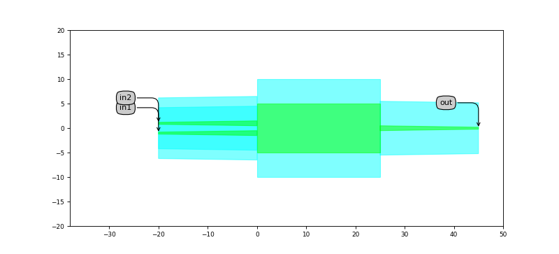
Ports
Name |
Type |
Position |
Angle |
Waveguide Template |
Inclination |
|---|---|---|---|---|---|
in1 |
Optical |
(-20.0,-1.0) |
180.0 |
RibWaveguideTemplate |
0.0 |
in2 |
Optical |
(-20.0,1.0) |
180.0 |
RibWaveguideTemplate |
0.0 |
out |
Optical |
(45.0,0.0) |
0.0 |
RibWaveguideTemplate |
0.0 |
Layout
Parameters
- port_width: float and number > 0
Width of port [um]
- taper_width: float and number > 0
Width of taper [um]
- mmi_width: float and number > 0
Width of the MMI [um]
- trace_spacing: float and Real, number and number >= 0
Offset between the traces at the input and the output
- length: float and number > 0
Length of the MMI
- transition_length: ( float and Real, number and number >= 0 ), None allowed
Length of the transition. Set to None to take the standard transition length.
RIB_2x2_MMI
PCell for 2x2 MMI in rib waveguide
- Parameters:
- transition_database: AutoTransitionDatabase
AutoTransitionDatabase in which the correct transition between the two trace templates can be looked up.
- port_labels: ( List with type restriction, allowed types: <class ‘str’> ), *None allowed*
Labels of the ports to be processed. Set to None to process all ports.
- external_port_names: str
Dictionary for remapping of the port names of the contents to the external ports
- name: String that contains only ISO/IEC 8859-1 (extended ASCII py3) or pure ASCII (py2) characters
The unique name of the pcell
- Other Parameters:
- input_trace_template: PCell and _TraceTemplate, locked
- mmi_trace_template: PCell and _TraceTemplate, locked
- output_trace_template: PCell and _TraceTemplate, locked
- trace_template: PCell and _TraceTemplate, locked
- transitions: List with type restriction, allowed types: <class ‘ipkiss3.pcell.cell.pcell.PCell’>, locked
- n_inputs: int and number > 0, locked
Number of input channels.
- n_outputs: int and number > 0, locked
Number of output channels.
- input_trace_templates: List with type restriction, allowed types: <class ‘ipkiss3.pcell.cell.pcell.PCell’>, locked
List of the input trace templates.
- output_trace_templates: List with type restriction, allowed types: <class ‘ipkiss3.pcell.cell.pcell.PCell’>, locked
List of the output trace templates.
- contents: PCell, locked
Contains the base MMI without the tapers
- mmi_trace: PCell, locked
Trace of the MMI section
- trace_templates: List with type restriction, allowed types: <class ‘ipkiss3.pcell.cell.pcell.PCell’>, locked
list of templates to apply to all ports
(Source code, png, hires.png, pdf)
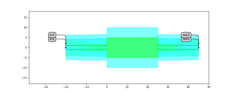
Ports
Name |
Type |
Position |
Angle |
Waveguide Template |
Inclination |
|---|---|---|---|---|---|
in1 |
Optical |
(-20.0,-1.0) |
180.0 |
RibWaveguideTemplate |
0.0 |
in2 |
Optical |
(-20.0,1.0) |
180.0 |
RibWaveguideTemplate |
0.0 |
out1 |
Optical |
(45.0,-1.0) |
0.0 |
RibWaveguideTemplate |
0.0 |
out2 |
Optical |
(45.0,1.0) |
0.0 |
RibWaveguideTemplate |
0.0 |
Layout
Parameters
- port_width: float and number > 0
Width of port [um]
- taper_width: float and number > 0
Width of taper [um]
- mmi_width: float and number > 0
Width of the MMI [um]
- trace_spacing: float and Real, number and number >= 0
Offset between the traces at the input and the output
- length: float and number > 0
Length of the MMI
- transition_length: ( float and Real, number and number >= 0 ), None allowed
Length of the transition. Set to None to take the standard transition length.
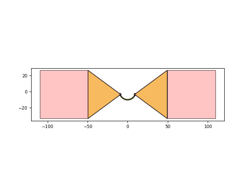
STRIP_2x1_MMI
PCell for 2x1 MMI in strip waveguide
- Parameters:
- transition_database: AutoTransitionDatabase
AutoTransitionDatabase in which the correct transition between the two trace templates can be looked up.
- port_labels: ( List with type restriction, allowed types: <class ‘str’> ), *None allowed*
Labels of the ports to be processed. Set to None to process all ports.
- external_port_names: str
Dictionary for remapping of the port names of the contents to the external ports
- name: String that contains only ISO/IEC 8859-1 (extended ASCII py3) or pure ASCII (py2) characters
The unique name of the pcell
- Other Parameters:
- input_trace_template: PCell and _TraceTemplate, locked
- mmi_trace_template: PCell and _TraceTemplate, locked
- output_trace_template: PCell and _TraceTemplate, locked
- trace_template: PCell and _TraceTemplate, locked
- transitions: List with type restriction, allowed types: <class ‘ipkiss3.pcell.cell.pcell.PCell’>, locked
- n_inputs: int and number > 0, locked
Number of input channels.
- n_outputs: int and number > 0, locked
Number of output channels.
- input_trace_templates: List with type restriction, allowed types: <class ‘ipkiss3.pcell.cell.pcell.PCell’>, locked
List of the input trace templates.
- output_trace_templates: List with type restriction, allowed types: <class ‘ipkiss3.pcell.cell.pcell.PCell’>, locked
List of the output trace templates.
- contents: PCell, locked
Contains the base MMI without the tapers
- mmi_trace: PCell, locked
Trace of the MMI section
- trace_templates: List with type restriction, allowed types: <class ‘ipkiss3.pcell.cell.pcell.PCell’>, locked
list of templates to apply to all ports
(Source code, png, hires.png, pdf)
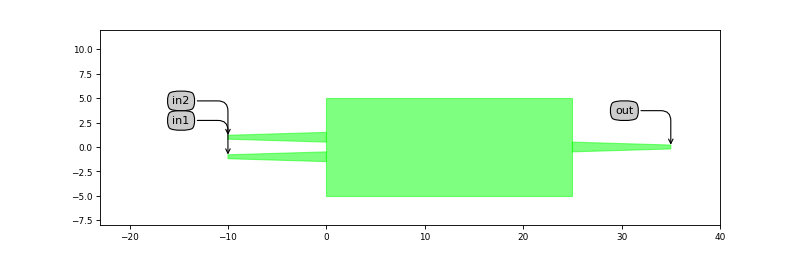
Ports
Name |
Type |
Position |
Angle |
Waveguide Template |
Inclination |
|---|---|---|---|---|---|
in1 |
Optical |
(-10.0,-1.0) |
180.0 |
StripWaveguideTemplate |
0.0 |
in2 |
Optical |
(-10.0,1.0) |
180.0 |
StripWaveguideTemplate |
0.0 |
out |
Optical |
(35.0,0.0) |
0.0 |
StripWaveguideTemplate |
0.0 |
Layout
Parameters
- port_width: float and number > 0
Width of port [um]
- taper_width: float and number > 0
Width of taper [um]
- mmi_width: float and number > 0
Width of the MMI [um]
- trace_spacing: float and Real, number and number >= 0
Offset between the traces at the input and the output
- length: float and number > 0
Length of the MMI
- transition_length: ( float and Real, number and number >= 0 ), None allowed
Length of the transition. Set to None to take the standard transition length.
STRIP_2x2_MMI
PCell for 2x2 MMI in strip waveguide
- Parameters:
- transition_database: AutoTransitionDatabase
AutoTransitionDatabase in which the correct transition between the two trace templates can be looked up.
- port_labels: ( List with type restriction, allowed types: <class ‘str’> ), *None allowed*
Labels of the ports to be processed. Set to None to process all ports.
- external_port_names: str
Dictionary for remapping of the port names of the contents to the external ports
- name: String that contains only ISO/IEC 8859-1 (extended ASCII py3) or pure ASCII (py2) characters
The unique name of the pcell
- Other Parameters:
- input_trace_template: PCell and _TraceTemplate, locked
- mmi_trace_template: PCell and _TraceTemplate, locked
- output_trace_template: PCell and _TraceTemplate, locked
- trace_template: PCell and _TraceTemplate, locked
- transitions: List with type restriction, allowed types: <class ‘ipkiss3.pcell.cell.pcell.PCell’>, locked
- n_inputs: int and number > 0, locked
Number of input channels.
- n_outputs: int and number > 0, locked
Number of output channels.
- input_trace_templates: List with type restriction, allowed types: <class ‘ipkiss3.pcell.cell.pcell.PCell’>, locked
List of the input trace templates.
- output_trace_templates: List with type restriction, allowed types: <class ‘ipkiss3.pcell.cell.pcell.PCell’>, locked
List of the output trace templates.
- contents: PCell, locked
Contains the base MMI without the tapers
- mmi_trace: PCell, locked
Trace of the MMI section
- trace_templates: List with type restriction, allowed types: <class ‘ipkiss3.pcell.cell.pcell.PCell’>, locked
list of templates to apply to all ports
(Source code, png, hires.png, pdf)
Ports
Name |
Type |
Position |
Angle |
Waveguide Template |
Inclination |
|---|---|---|---|---|---|
in1 |
Optical |
(-10.0,-1.0) |
180.0 |
StripWaveguideTemplate |
0.0 |
in2 |
Optical |
(-10.0,1.0) |
180.0 |
StripWaveguideTemplate |
0.0 |
out1 |
Optical |
(35.0,-1.0) |
0.0 |
StripWaveguideTemplate |
0.0 |
out2 |
Optical |
(35.0,1.0) |
0.0 |
StripWaveguideTemplate |
0.0 |
Layout
Parameters
- port_width: float and number > 0
Width of port [um]
- taper_width: float and number > 0
Width of taper [um]
- mmi_width: float and number > 0
Width of the MMI [um]
- trace_spacing: float and Real, number and number >= 0
Offset between the traces at the input and the output
- length: float and number > 0
Length of the MMI
- transition_length: ( float and Real, number and number >= 0 ), None allowed
Length of the transition. Set to None to take the standard transition length.
220 nm SOI cells
SOI220nm_1550nm_TE_RIB_2X1_MMI
C-band 50/50 splitting 2x1 rib MMI
Ports
Name |
Type |
Position |
Angle |
Waveguide Template |
Inclination |
|---|---|---|---|---|---|
in1 |
Optical |
(-20.0,-1.57) |
180.0 |
RibWaveguideTemplate |
0.0 |
in2 |
Optical |
(-20.0,1.57) |
180.0 |
RibWaveguideTemplate |
0.0 |
out |
Optical |
(52.7,0.0) |
0.0 |
RibWaveguideTemplate |
0.0 |
SOI220nm_1550nm_TE_RIB_2x2_MMI
C-band 50/50 splitting 2x2 rib MMI
Ports
Name |
Type |
Position |
Angle |
Waveguide Template |
Inclination |
|---|---|---|---|---|---|
in1 |
Optical |
(-20.0,-1.015) |
180.0 |
RibWaveguideTemplate |
0.0 |
in2 |
Optical |
(-20.0,1.015) |
180.0 |
RibWaveguideTemplate |
0.0 |
out1 |
Optical |
(64.8,-1.015) |
0.0 |
RibWaveguideTemplate |
0.0 |
out2 |
Optical |
(64.8,1.015) |
0.0 |
RibWaveguideTemplate |
0.0 |
SOI220nm_1550nm_TE_STRIP_2X1_MMI
C-band 50/50 splitting 2x1 strip MMI
Ports
Name |
Type |
Position |
Angle |
Waveguide Template |
Inclination |
|---|---|---|---|---|---|
in1 |
Optical |
(-20.0,-1.57) |
180.0 |
StripWaveguideTemplate |
0.0 |
in2 |
Optical |
(-20.0,1.57) |
180.0 |
StripWaveguideTemplate |
0.0 |
out |
Optical |
(51.8,0.0) |
0.0 |
StripWaveguideTemplate |
0.0 |
SOI220nm_1550nm_TE_STRIP_2x2_MMI
C-band 50/50 splitting 2x2 strip MMI
Ports
Name |
Type |
Position |
Angle |
Waveguide Template |
Inclination |
|---|---|---|---|---|---|
in1 |
Optical |
(-20.0,-1.015) |
180.0 |
StripWaveguideTemplate |
0.0 |
in2 |
Optical |
(-20.0,1.015) |
180.0 |
StripWaveguideTemplate |
0.0 |
out1 |
Optical |
(62.5,-1.015) |
0.0 |
StripWaveguideTemplate |
0.0 |
out2 |
Optical |
(62.5,1.015) |
0.0 |
StripWaveguideTemplate |
0.0 |
SOI220nm_1310nm_TE_RIB_2X1_MMI
O-band 50/50 splitting 2x1 rib MMI
Ports
Name |
Type |
Position |
Angle |
Waveguide Template |
Inclination |
|---|---|---|---|---|---|
in1 |
Optical |
(-20.0,-1.525) |
180.0 |
RibWaveguideTemplate |
0.0 |
in2 |
Optical |
(-20.0,1.525) |
180.0 |
RibWaveguideTemplate |
0.0 |
out |
Optical |
(60.8,0.0) |
0.0 |
RibWaveguideTemplate |
0.0 |
SOI220nm_1310nm_TE_RIB_2x2_MMI
O-band 50/50 splitting 2x2 rib MMI
Ports
Name |
Type |
Position |
Angle |
Waveguide Template |
Inclination |
|---|---|---|---|---|---|
in1 |
Optical |
(-20.0,-1.015) |
180.0 |
RibWaveguideTemplate |
0.0 |
in2 |
Optical |
(-20.0,1.015) |
180.0 |
RibWaveguideTemplate |
0.0 |
out1 |
Optical |
(75.0,-1.015) |
0.0 |
RibWaveguideTemplate |
0.0 |
out2 |
Optical |
(75.0,1.015) |
0.0 |
RibWaveguideTemplate |
0.0 |
SOI220nm_1310nm_TE_STRIP_2X1_MMI
O-band 50/50 splitting 2x1 strip MMI
Ports
Name |
Type |
Position |
Angle |
Waveguide Template |
Inclination |
|---|---|---|---|---|---|
in1 |
Optical |
(-20.0,-1.525) |
180.0 |
StripWaveguideTemplate |
0.0 |
in2 |
Optical |
(-20.0,1.525) |
180.0 |
StripWaveguideTemplate |
0.0 |
out |
Optical |
(60.1,0.0) |
0.0 |
StripWaveguideTemplate |
0.0 |
SOI220nm_1310nm_TE_STRIP_2x2_MMI
O-band 50/50 splitting 2x2 strip MMI
Ports
Name |
Type |
Position |
Angle |
Waveguide Template |
Inclination |
|---|---|---|---|---|---|
in1 |
Optical |
(-20.0,-1.015) |
180.0 |
StripWaveguideTemplate |
0.0 |
in2 |
Optical |
(-20.0,1.015) |
180.0 |
StripWaveguideTemplate |
0.0 |
out1 |
Optical |
(73.5,-1.015) |
0.0 |
StripWaveguideTemplate |
0.0 |
out2 |
Optical |
(73.5,1.015) |
0.0 |
StripWaveguideTemplate |
0.0 |
340 nm SOI cells
SOI340nm_1550nm_TE_RIB_2X1_MMI
C-band 50/50 splitting 2x1 MMI
Ports
Name |
Type |
Position |
Angle |
Waveguide Template |
Inclination |
|---|---|---|---|---|---|
in1 |
Optical |
(-20.0,-1.525) |
180.0 |
RibWaveguideTemplate |
0.0 |
in2 |
Optical |
(-20.0,1.525) |
180.0 |
RibWaveguideTemplate |
0.0 |
out |
Optical |
(56.0,0.0) |
0.0 |
RibWaveguideTemplate |
0.0 |
SOI340nm_1550nm_TE_RIB_2X2_MMI
C-band 50/50 splitting 2x2 MMI
Ports
Name |
Type |
Position |
Angle |
Waveguide Template |
Inclination |
|---|---|---|---|---|---|
in1 |
Optical |
(-20.0,-1.015) |
180.0 |
RibWaveguideTemplate |
0.0 |
in2 |
Optical |
(-20.0,1.015) |
180.0 |
RibWaveguideTemplate |
0.0 |
out1 |
Optical |
(69.0,-1.015) |
0.0 |
RibWaveguideTemplate |
0.0 |
out2 |
Optical |
(69.0,1.015) |
0.0 |
RibWaveguideTemplate |
0.0 |
SOI340nm_1550nm_TE_STRIP_2X1_MMI
C-band 50/50 splitting strip 2x1 MMI
Ports
Name |
Type |
Position |
Angle |
Waveguide Template |
Inclination |
|---|---|---|---|---|---|
in1 |
Optical |
(-20.0,-1.575) |
180.0 |
StripWaveguideTemplate |
0.0 |
in2 |
Optical |
(-20.0,1.575) |
180.0 |
StripWaveguideTemplate |
0.0 |
out |
Optical |
(54.7,0.0) |
0.0 |
StripWaveguideTemplate |
0.0 |
SOI340nm_1550nm_TE_STRIP_2X2_MMI
C-band 50/50 splitting strip 2x2 MMI
Ports
Name |
Type |
Position |
Angle |
Waveguide Template |
Inclination |
|---|---|---|---|---|---|
in1 |
Optical |
(-20.0,-1.015) |
180.0 |
StripWaveguideTemplate |
0.0 |
in2 |
Optical |
(-20.0,1.015) |
180.0 |
StripWaveguideTemplate |
0.0 |
out1 |
Optical |
(66.5,-1.015) |
0.0 |
StripWaveguideTemplate |
0.0 |
out2 |
Optical |
(66.5,1.015) |
0.0 |
StripWaveguideTemplate |
0.0 |
SOI340nm_1310nm_TE_RIB_2X1_MMI
O-band 50/50 splitting 2x1 MMI
Ports
Name |
Type |
Position |
Angle |
Waveguide Template |
Inclination |
|---|---|---|---|---|---|
in1 |
Optical |
(-20.0,-1.505) |
180.0 |
RibWaveguideTemplate |
0.0 |
in2 |
Optical |
(-20.0,1.505) |
180.0 |
RibWaveguideTemplate |
0.0 |
out |
Optical |
(63.7,0.0) |
0.0 |
RibWaveguideTemplate |
0.0 |
SOI340nm_1310nm_TE_RIB_2X2_MMI
O-band 50/50 splitting 2x2 MMI
Ports
Name |
Type |
Position |
Angle |
Waveguide Template |
Inclination |
|---|---|---|---|---|---|
in1 |
Optical |
(-20.0,-1.015) |
180.0 |
RibWaveguideTemplate |
0.0 |
in2 |
Optical |
(-20.0,1.015) |
180.0 |
RibWaveguideTemplate |
0.0 |
out1 |
Optical |
(78.3,-1.015) |
0.0 |
RibWaveguideTemplate |
0.0 |
out2 |
Optical |
(78.3,1.015) |
0.0 |
RibWaveguideTemplate |
0.0 |
SOI340nm_1310nm_TE_STRIP_2X1_MMI
O-band 50/50 splitting strip 2x1 MMI
Ports
Name |
Type |
Position |
Angle |
Waveguide Template |
Inclination |
|---|---|---|---|---|---|
in1 |
Optical |
(-20.0,-1.505) |
180.0 |
StripWaveguideTemplate |
0.0 |
in2 |
Optical |
(-20.0,1.505) |
180.0 |
StripWaveguideTemplate |
0.0 |
out |
Optical |
(62.6,0.0) |
0.0 |
StripWaveguideTemplate |
0.0 |
SOI340nm_1310nm_TE_STRIP_2X2_MMI
O-band 50/50 splitting strip 2x2 MMI
Ports
Name |
Type |
Position |
Angle |
Waveguide Template |
Inclination |
|---|---|---|---|---|---|
in1 |
Optical |
(-20.0,-1.0) |
180.0 |
StripWaveguideTemplate |
0.0 |
in2 |
Optical |
(-20.0,1.0) |
180.0 |
StripWaveguideTemplate |
0.0 |
out1 |
Optical |
(77.0,-1.0) |
0.0 |
StripWaveguideTemplate |
0.0 |
out2 |
Optical |
(77.0,1.0) |
0.0 |
StripWaveguideTemplate |
0.0 |
500 nm SOI cells
SOI500nm_1550nm_TE_RIB_2X1_MMI
C-band 50/50 splitting 2x1 MMI
Ports
Name |
Type |
Position |
Angle |
Waveguide Template |
Inclination |
|---|---|---|---|---|---|
in1 |
Optical |
(-20.0,-1.535) |
180.0 |
RibWaveguideTemplate |
0.0 |
in2 |
Optical |
(-20.0,1.535) |
180.0 |
RibWaveguideTemplate |
0.0 |
out |
Optical |
(57.5,0.0) |
0.0 |
RibWaveguideTemplate |
0.0 |
SOI500nm_1550nm_TE_RIB_2X2_MMI
C-band 50/50 splitting 2x2 MMI
Ports
Name |
Type |
Position |
Angle |
Waveguide Template |
Inclination |
|---|---|---|---|---|---|
in1 |
Optical |
(-20.0,-1.0) |
180.0 |
RibWaveguideTemplate |
0.0 |
in2 |
Optical |
(-20.0,1.0) |
180.0 |
RibWaveguideTemplate |
0.0 |
out1 |
Optical |
(70.2,-1.0) |
0.0 |
RibWaveguideTemplate |
0.0 |
out2 |
Optical |
(70.2,1.0) |
0.0 |
RibWaveguideTemplate |
0.0 |
Crossings
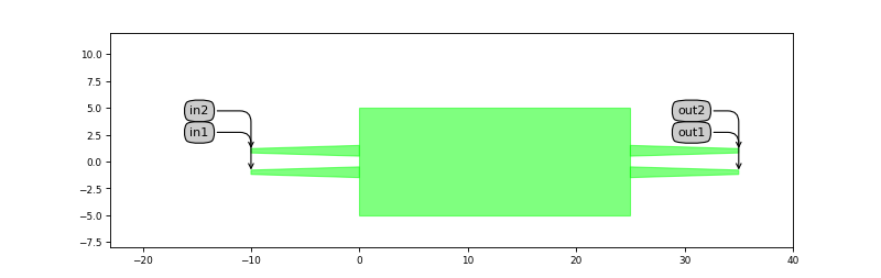
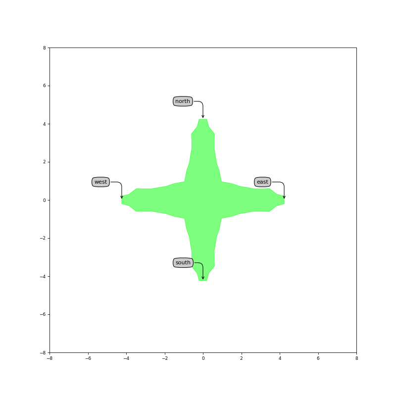
SOI220nm_1550nm_TE_RIB_Waveguide_Crossing
Waveguide crossing in rib waveguide for the C band
(Source code, png, hires.png, pdf)
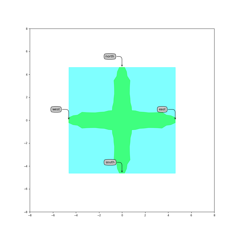
Ports
Name |
Type |
Position |
Angle |
Waveguide Template |
Inclination |
|---|---|---|---|---|---|
east |
Optical |
(4.62,0.0) |
0.0 |
RibWaveguideTemplate |
0.0 |
north |
Optical |
(0.0,4.62) |
90.0 |
RibWaveguideTemplate |
0.0 |
west |
Optical |
(-4.62,0.0) |
180.0 |
RibWaveguideTemplate |
0.0 |
south |
Optical |
(0.0,-4.62) |
-90.0 |
RibWaveguideTemplate |
0.0 |
SOI220nm_1310nm_TE_RIB_Waveguide_Crossing
Waveguide crossing in rib waveguide for the O band
(Source code, png, hires.png, pdf)
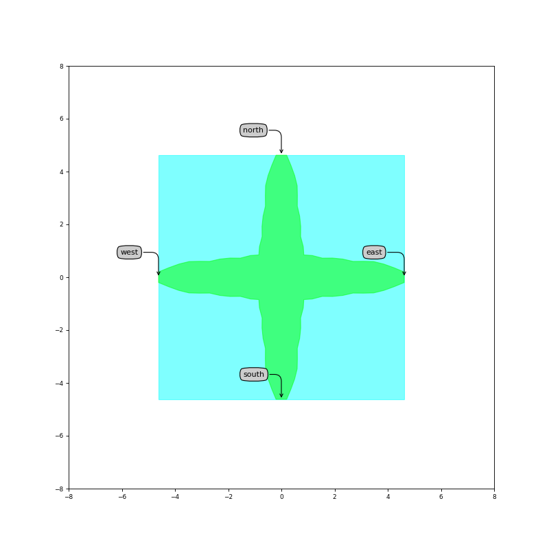
Ports
Name |
Type |
Position |
Angle |
Waveguide Template |
Inclination |
|---|---|---|---|---|---|
east |
Optical |
(4.62,0.0) |
0.0 |
RibWaveguideTemplate |
0.0 |
north |
Optical |
(0.0,4.62) |
90.0 |
RibWaveguideTemplate |
0.0 |
west |
Optical |
(-4.62,0.0) |
180.0 |
RibWaveguideTemplate |
0.0 |
south |
Optical |
(0.0,-4.62) |
-90.0 |
RibWaveguideTemplate |
0.0 |
SOI220nm_1550nm_TE_STRIP_Waveguide_Crossing
Waveguide crossing in strip waveguide for the C band
(Source code, png, hires.png, pdf)
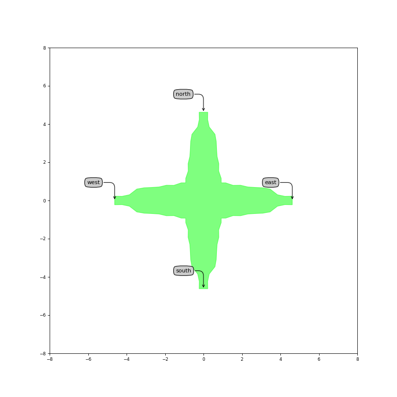
Ports
Name |
Type |
Position |
Angle |
Waveguide Template |
Inclination |
|---|---|---|---|---|---|
east |
Optical |
(4.62,0.0) |
0.0 |
StripWaveguideTemplate |
0.0 |
north |
Optical |
(0.0,4.62) |
90.0 |
StripWaveguideTemplate |
0.0 |
west |
Optical |
(-4.62,0.0) |
180.0 |
StripWaveguideTemplate |
0.0 |
south |
Optical |
(0.0,-4.62) |
-90.0 |
StripWaveguideTemplate |
0.0 |
SOI220nm_1310nm_TE_STRIP_Waveguide_Crossing
Waveguide crossing in strip waveguide for the O band
(Source code, png, hires.png, pdf)
Ports
Name |
Type |
Position |
Angle |
Waveguide Template |
Inclination |
|---|---|---|---|---|---|
east |
Optical |
(4.235,0.0) |
0.0 |
StripWaveguideTemplate |
0.0 |
north |
Optical |
(0.0,4.235) |
90.0 |
StripWaveguideTemplate |
0.0 |
west |
Optical |
(-4.235,0.0) |
180.0 |
StripWaveguideTemplate |
0.0 |
south |
Optical |
(0.0,-4.235) |
-90.0 |
StripWaveguideTemplate |
0.0 |
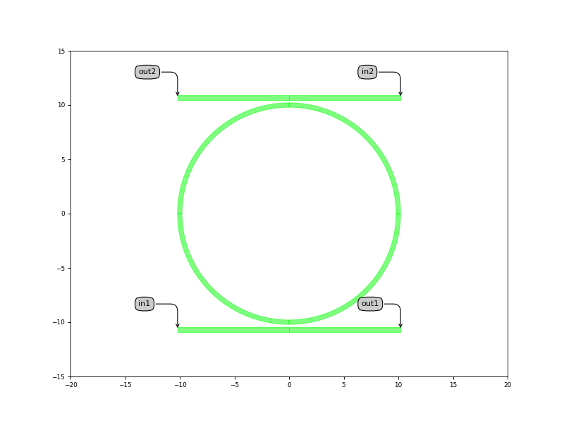
Ring Filters
RIB_AllPass_Ring
PCell for All-Pass Ring filter in rib wavegudie
- Parameters:
- coupler_trace_templates: List with type restriction, allowed types: <class ‘ipkiss3.pcell.cell.pcell.PCell’>
list of trace_templates for the ring couplers. By default the same template as the ring is taken
- ring_trace_template: PCell and _WaveguideTemplate
Trace template for the ring waveguide
- couplers: List with type restriction, allowed types: <class ‘ipkiss3.pcell.cell.pcell.PCell’>
list of coupler PCells
- ring_segments: List with type restriction, allowed types: <class ‘ipkiss3.pcell.cell.pcell.PCell’>
list of Ring PCells
- name: String that contains only ISO/IEC 8859-1 (extended ASCII py3) or pure ASCII (py2) characters
The unique name of the pcell
- Other Parameters:
- ring_trace_templates: List with type restriction, allowed types: <class ‘ipkiss3.pcell.cell.pcell.PCell’>, locked
Trace templates for the ring segments. Locked, as there is only one segment in this Ring. Use ‘ring_trace_template’ instead.
(Source code, png, hires.png, pdf)
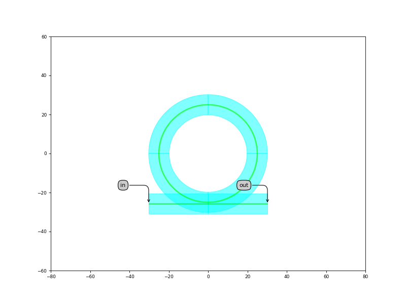
Ports
Name |
Type |
Position |
Angle |
Waveguide Template |
Inclination |
|---|---|---|---|---|---|
in |
Optical |
(-30.2,-25.68) |
180.0 |
RibWaveguideTemplate |
0.0 |
out |
Optical |
(30.2,-25.68) |
0.0 |
RibWaveguideTemplate |
0.0 |
Layout
Parameters
- coupler_length: float and Real, number and number >= 0
Straight coupling part length [um]
- coupler_spacing: float and number > 0
Centerline-to-centerline spacing of the coupler [um]
- ring_length: float and number > 0
Total ring length (min of 2 * (pi*bend_radius + coupler_length))[um]
- width: float and number > 0
Width of the waveguide [um]
- bend_radius: float and number > 0
Bend radius for the auto-generated bends.
RIB_AddDrop_Ring
PCell for Add-Drop Ring filter in rib wavegudie
- Parameters:
- coupler_trace_templates: List with type restriction, allowed types: <class ‘ipkiss3.pcell.cell.pcell.PCell’>
list of trace_templates for the ring couplers. By default the same template as the ring is taken
- ring_trace_template: PCell and _WaveguideTemplate
Trace template for the ring waveguide
- couplers: List with type restriction, allowed types: <class ‘ipkiss3.pcell.cell.pcell.PCell’>
list of coupler PCells
- ring_segments: List with type restriction, allowed types: <class ‘ipkiss3.pcell.cell.pcell.PCell’>
list of Ring PCells
- name: String that contains only ISO/IEC 8859-1 (extended ASCII py3) or pure ASCII (py2) characters
The unique name of the pcell
- Other Parameters:
- ring_trace_templates: List with type restriction, allowed types: <class ‘ipkiss3.pcell.cell.pcell.PCell’>, locked
Trace templates for the ring segments. Locked, as there is only one segment in this Ring. Use ‘ring_trace_template’ instead.
(Source code, png, hires.png, pdf)
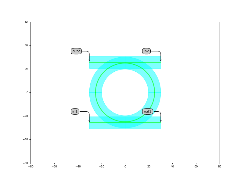
Ports
Name |
Type |
Position |
Angle |
Waveguide Template |
Inclination |
|---|---|---|---|---|---|
in1 |
Optical |
(-30.2,-25.68) |
180.0 |
RibWaveguideTemplate |
0.0 |
out1 |
Optical |
(30.2,-25.68) |
0.0 |
RibWaveguideTemplate |
0.0 |
in2 |
Optical |
(30.2,25.68) |
0.0 |
RibWaveguideTemplate |
0.0 |
out2 |
Optical |
(-30.2,25.68) |
180.0 |
RibWaveguideTemplate |
0.0 |
Layout
Parameters
- bottom_coupler_spacing: float and number > 0
Centerline-to-centerline spacing of the bottom coupler [um]
- coupler_length: float and Real, number and number >= 0
Straight coupling length [um]
- ring_length: float and number > 0
Total ring length (min of 2 * (pi*bend_radius + coupler_length))[um]
- top_coupler_spacing: float and number > 0
Centerline-to-centerline spacing of the top coupler [um]
- width: float and number > 0
Width of the waveguide [um]
- bend_radius: float and number > 0
Bend radius for the auto-generated bends.
STRIP_AllPass_Ring
PCell for All-Pass Ring filter in strip waveguide
- Parameters:
- coupler_trace_templates: List with type restriction, allowed types: <class ‘ipkiss3.pcell.cell.pcell.PCell’>
list of trace_templates for the ring couplers. By default the same template as the ring is taken
- ring_trace_template: PCell and _WaveguideTemplate
Trace template for the ring waveguide
- couplers: List with type restriction, allowed types: <class ‘ipkiss3.pcell.cell.pcell.PCell’>
list of coupler PCells
- ring_segments: List with type restriction, allowed types: <class ‘ipkiss3.pcell.cell.pcell.PCell’>
list of Ring PCells
- name: String that contains only ISO/IEC 8859-1 (extended ASCII py3) or pure ASCII (py2) characters
The unique name of the pcell
- Other Parameters:
- ring_trace_templates: List with type restriction, allowed types: <class ‘ipkiss3.pcell.cell.pcell.PCell’>, locked
Trace templates for the ring segments. Locked, as there is only one segment in this Ring. Use ‘ring_trace_template’ instead.
(Source code, png, hires.png, pdf)
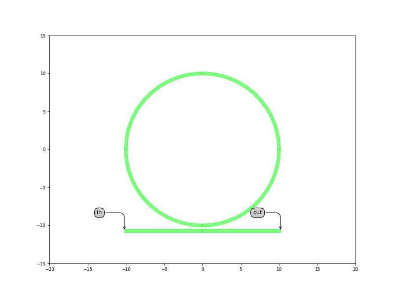
Ports
Name |
Type |
Position |
Angle |
Waveguide Template |
Inclination |
|---|---|---|---|---|---|
in |
Optical |
(-10.2,-10.68) |
180.0 |
StripWaveguideTemplate |
0.0 |
out |
Optical |
(10.2,-10.68) |
0.0 |
StripWaveguideTemplate |
0.0 |
Layout
Parameters
- coupler_length: float and Real, number and number >= 0
Straight coupling part length [um]
- coupler_spacing: float and number > 0
Centerline-to-centerline spacing of the coupler [um]
- ring_length: float and number > 0
Total ring length (min of 2 * (pi*bend_radius + coupler_length))[um]
- width: float and number > 0
Width of the waveguide [um]
- bend_radius: float and number > 0
Bend radius for the auto-generated bends.
STRIP_AddDrop_Ring
PCell for Add-Drop Ring filter in strip waveguide
- Parameters:
- coupler_trace_templates: List with type restriction, allowed types: <class ‘ipkiss3.pcell.cell.pcell.PCell’>
list of trace_templates for the ring couplers. By default the same template as the ring is taken
- ring_trace_template: PCell and _WaveguideTemplate
Trace template for the ring waveguide
- couplers: List with type restriction, allowed types: <class ‘ipkiss3.pcell.cell.pcell.PCell’>
list of coupler PCells
- ring_segments: List with type restriction, allowed types: <class ‘ipkiss3.pcell.cell.pcell.PCell’>
list of Ring PCells
- name: String that contains only ISO/IEC 8859-1 (extended ASCII py3) or pure ASCII (py2) characters
The unique name of the pcell
- Other Parameters:
- ring_trace_templates: List with type restriction, allowed types: <class ‘ipkiss3.pcell.cell.pcell.PCell’>, locked
Trace templates for the ring segments. Locked, as there is only one segment in this Ring. Use ‘ring_trace_template’ instead.
(Source code, png, hires.png, pdf)
Ports
Name |
Type |
Position |
Angle |
Waveguide Template |
Inclination |
|---|---|---|---|---|---|
in1 |
Optical |
(-10.2,-10.68) |
180.0 |
StripWaveguideTemplate |
0.0 |
out1 |
Optical |
(10.2,-10.68) |
0.0 |
StripWaveguideTemplate |
0.0 |
in2 |
Optical |
(10.2,10.68) |
0.0 |
StripWaveguideTemplate |
0.0 |
out2 |
Optical |
(-10.2,10.68) |
180.0 |
StripWaveguideTemplate |
0.0 |
Layout
Parameters
- bottom_coupler_spacing: float and number > 0
Centerline-to-centerline spacing of the bottom coupler [um]
- coupler_length: float and Real, number and number >= 0
Straight coupling length [um]
- ring_length: float and number > 0
Total ring length (min of 2 * (pi*bend_radius + coupler_length))[um]
- top_coupler_spacing: float and number > 0
Centerline-to-centerline spacing of the top coupler [um]
- width: float and number > 0
Width of the waveguide [um]
- bend_radius: float and number > 0
Bend radius for the auto-generated bends.
Modulators
SOI220nm_1550nm_TE_MZI_Modulator
Mach-Zehnder Modulator with fixed dimensions in rib waveguide for the C band
(Source code, png, hires.png, pdf)
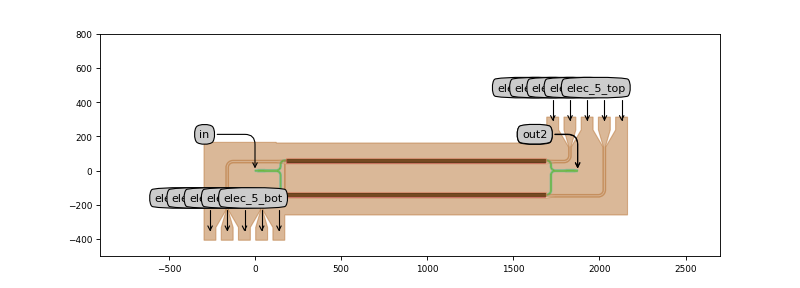
Ports
Name |
Type |
Position |
Angle |
Waveguide Template |
Inclination |
|---|---|---|---|---|---|
in |
Optical |
(0.0,0.0) |
180.0 |
RibWaveguideTemplate |
0.0 |
out1 |
Optical |
(1873.4,-1.015) |
0.0 |
RibWaveguideTemplate |
0.0 |
out2 |
Optical |
(1873.4,1.015) |
0.0 |
RibWaveguideTemplate |
0.0 |
elec_1_bot |
Electrical |
(-260.8,-369.05) |
None |
ElectricalWireTemplate |
0.0 |
elec_2_bot |
Electrical |
(-160.8,-369.05) |
None |
ElectricalWireTemplate |
0.0 |
elec_3_bot |
Electrical |
(-60.8,-369.05) |
None |
ElectricalWireTemplate |
0.0 |
elec_4_bot |
Electrical |
(39.2,-369.05) |
None |
ElectricalWireTemplate |
0.0 |
elec_5_bot |
Electrical |
(139.2,-369.05) |
None |
ElectricalWireTemplate |
0.0 |
elec_1_top |
Electrical |
(1729.2,275.95) |
None |
ElectricalWireTemplate |
0.0 |
elec_2_top |
Electrical |
(1829.2,275.95) |
None |
ElectricalWireTemplate |
0.0 |
elec_3_top |
Electrical |
(1929.2,275.95) |
None |
ElectricalWireTemplate |
0.0 |
elec_4_top |
Electrical |
(2029.2,275.95) |
None |
ElectricalWireTemplate |
0.0 |
elec_5_top |
Electrical |
(2129.2,275.95) |
None |
ElectricalWireTemplate |
0.0 |
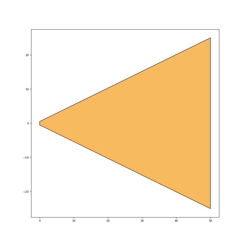
RIB_Modulator
Rib Modulator with parameters to set up the implants and the metal.
- Parameters:
- name: String that contains only ISO/IEC 8859-1 (extended ASCII py3) or pure ASCII (py2) characters
The unique name of the pcell
(Source code, png, hires.png, pdf)
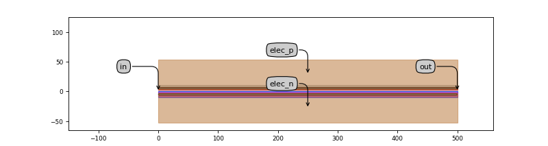
Ports
Name |
Type |
Position |
Angle |
Waveguide Template |
Inclination |
|---|---|---|---|---|---|
in |
Optical |
(0.0,0.0) |
180.0 |
RibWaveguideTemplate |
0.0 |
out |
Optical |
(500.0,0.0) |
0.0 |
RibWaveguideTemplate |
0.0 |
elec_n |
Electrical |
(250.0,-28.35) |
None |
ElectricalWireTemplate |
0.0 |
elec_p |
Electrical |
(250.0,28.35) |
None |
ElectricalWireTemplate |
0.0 |
Layout
Parameters
- core_width: float and number > 0
width of the core
- high_dose_n_offset: float
offset from the center line of high dose N implant
- high_dose_n_width: float and number > 0
width of high dose N implant
- high_dose_p_offset: float
offset from the center line of high dose P implant
- high_dose_p_width: float and number > 0
width of high dose P implant
- length: float and number > 0
length of the PN junction
- m1_n_offset: float
offset from the center line of metal on the N implant
- m1_n_width: float and number > 0
width of metal on the N implant
- m1_p_offset: float
offset from the center line of metal on the P implant
- m1_p_width: float and number > 0
width of metal on the P implant
- n_offset: float
offset from the center line of low dose N implant
- n_width: float and number > 0
width of low dose N implant
- p_offset: float
offset from the center line of low dose P implant
- p_width: float and number > 0
width of low dose P implant
- slab_width: float and number > 0
width of the slab
- via_n_offset: float
offset from the center line of vias etch on N implant
- via_p_offset: float
offset from the center line of vias etch on P implant
- via_width: float and number > 0
width of vias etch (same on both side of the center line)
Heaters
A number of parametric cells are defined to assist the designer in creating heater filaments and metallization:
HeaterFilament
- Parameters:
- trace_template: PCell and ElectricalWireTemplate
(Source code, png, hires.png, pdf)
Ports
Name |
Type |
Position |
Angle |
Waveguide Template |
Inclination |
|---|---|---|---|---|---|
in |
Electrical |
(0.45,0.0) |
None |
HeaterFilamentTemplate |
0.0 |
out |
Electrical |
(99.55,-0.0) |
None |
HeaterFilamentTemplate |
0.0 |
Layout
Parameters
- shape: Shape
Shape from which the Trace is calculated
Examples
import cornerstone.all as cornerstone_lib
import ipkiss3.all as i3
from picazzo3.routing.place_route import PlaceComponents

filament = cornerstone_lib.HeaterFilament()
filament_sh = i3.ShapeArc(radius=10.0, start_angle=200.0, end_angle=340.0)
filament.Layout(shape=filament_sh)

contact_wedge = cornerstone_lib.HeaterWedge()
contact_wedge.Layout(end_width=60.0, length=40.0)

contact_pad = cornerstone_lib.HeaterPad()
contact_pad.Layout(height=60.0, width=60.0)

contacted_heater = PlaceComponents(
    name="contacted_heater",
    child_cells={
        "filament": filament,
        "wedge_west": contact_wedge,
        "wedge_east": contact_wedge,
        "pad_west": contact_pad,
        "pad_east": contact_pad,
    },
)
contacted_heater_lo = contacted_heater.Layout(
    child_transformations={
        "filament": (0.0, 0.0),
        "wedge_west": i3.Rotation(rotation=180.0) + i3.Translation(filament_sh[0]),
        "pad_west": filament_sh[0] - i3.Coord2((70.0, 0.0)),
        "wedge_east": filament_sh[-1],
        "pad_east": filament_sh[-1] + i3.Coord2((70.0, 0.0)),
    }
)

contacted_heater_lo.visualize()
(Source code, png, hires.png, pdf)
StraightHeaterFilament
- Parameters:
- trace_template: PCell and ElectricalWireTemplate
(Source code, png, hires.png, pdf)
Ports
Name |
Type |
Position |
Angle |
Waveguide Template |
Inclination |
|---|---|---|---|---|---|
in |
Electrical |
(0.45,0.0) |
None |
HeaterFilamentTemplate |
0.0 |
out |
Electrical |
(99.55,-0.0) |
None |
HeaterFilamentTemplate |
0.0 |
HeaterWedge
- Parameters:
- name: String that contains only ISO/IEC 8859-1 (extended ASCII py3) or pure ASCII (py2) characters
The unique name of the pcell
(Source code, png, hires.png, pdf)
Layout
Parameters
- end_width: float and number > 0
End width of the Wedge [um]
- length: float and number > 0
Length of the Wedge [um]
- tip_width: float and number > 0
Tip width of the Wedge [um]
HeaterPad
- Parameters:
- name: String that contains only ISO/IEC 8859-1 (extended ASCII py3) or pure ASCII (py2) characters
The unique name of the pcell
(Source code, png, hires.png, pdf)
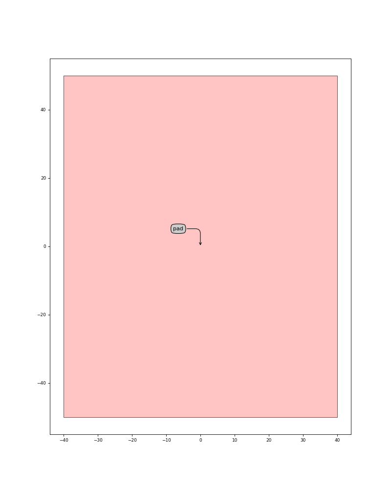
Ports
Name |
Type |
Position |
Angle |
Waveguide Template |
Inclination |
|---|---|---|---|---|---|
pad |
Electrical |
(0.0,0.0) |
None |
ElectricalWireTemplate |
0.0 |
Layout
Parameters
- height: float and number > 0
Height of the pad [um]
- width: float and number > 0
Width of the pad [um]
Y-Splitters
Ysplitter
PCell for Y-splitter.
- Parameters:
- trace_template: PCell and _WaveguideTemplate
Trace template of the Y-splitter (Strip by default)
(Source code, png, hires.png, pdf)
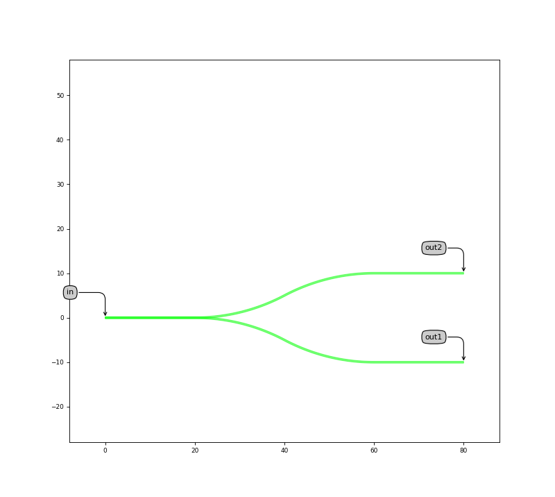
Ports
Name |
Type |
Position |
Angle |
Waveguide Template |
Inclination |
|---|---|---|---|---|---|
in |
Optical |
(0.0,0.0) |
180.0 |
StripWaveguideTemplate |
0.0 |
out1 |
Optical |
(80.0,-10.0) |
0.0 |
StripWaveguideTemplate |
0.0 |
out2 |
Optical |
(80.0,10.0) |
0.0 |
StripWaveguideTemplate |
0.0 |
Layout
Parameters
- length: float and number > 0
Length of sbend [um]
- straight_length: float and number > 0
Length of straight sections [um]
- width: float and number > 0
Width of the waveguide (only used if no trace_template provided) [um]
220 nm SOI cells
SOI220nm_1550nm_TE_STRIP_2x1_Ysplitter
TE Y splitter in strip waveguide for the C band
Ports
Name |
Type |
Position |
Angle |
Waveguide Template |
Inclination |
|---|---|---|---|---|---|
in |
Optical |
(0.0,0.0) |
180.0 |
StripWaveguideTemplate |
0.0 |
out1 |
Optical |
(80.0,-10.0) |
0.0 |
StripWaveguideTemplate |
0.0 |
out2 |
Optical |
(80.0,10.0) |
0.0 |
StripWaveguideTemplate |
0.0 |
SOI220nm_1310nm_TE_STRIP_2x1_Ysplitter
TE Y splitter in strip waveguide for the O band
Ports
Name |
Type |
Position |
Angle |
Waveguide Template |
Inclination |
|---|---|---|---|---|---|
in |
Optical |
(0.0,0.0) |
180.0 |
StripWaveguideTemplate |
0.0 |
out1 |
Optical |
(80.0,-10.0) |
0.0 |
StripWaveguideTemplate |
0.0 |
out2 |
Optical |
(80.0,10.0) |
0.0 |
StripWaveguideTemplate |
0.0 |