
Luceda PDK for SiEPIC Shuksan
The Luceda PDK for SiEPIC Shuksan allows to design and tape out to the first ever laser integration multi-project wafer (MPW) run offered by SiEPICfab.
Contents
PDK Documentation
This document explains how to use the Luceda Process Design Kit (PDK) for SiEPICfab (version 0.2.3.luceda4).
The PDK can be used from Luceda IPKISS, providing the following functionality:
definition and layout of circuits using SiEPIC’s predefined library of cells (building blocks), which is entirely available within IPKISS,
waveguide routing using the waveguide types defined, or custom defined waveguides following design rules,
definition of custom devices using defined layers and design rules,
simulation of custom devices using IPKISS’ built-in solvers and IPKISS Links to 3rd party tools such as Dassault Systemes Simulia CST Studio Suite ® and Ansys Lumerical FDTD,
circuit editing from Siemens L-Edit using Luceda Link for Siemens EDA.
This documentation explains how to get started with the PDK, lists the cells that are available and documents the technology for custom design.
Document information
This PDK is an implementation of SiEPICfab’s PDK.
License
The GDSII library source files from SiEPIC Shuksan GitHub PDK, replicated here under the
siepic_shuksan/ipkiss/siepic_shuksan/gdsdirectory, are distributed under the terms of an MIT license.Other than these original GDSII files, all files in this PDK implementation are copyrighted by Luceda Photonics © 2021, under the following terms and conditions:
This version of Luceda Academy and related packages
(hereafter referred to as Luceda Academy) is distributed under a proprietary License by Luceda.
It does allow you to develop and distribute add-ons or plug-ins, but does
not allow redistribution of Luceda Academy  itself (in original or modified form).

This program is distributed in the hope that it will be useful, but WITHOUT
ANY WARRANTY; without even the implied warranty of MERCHANTABILITY or FITNESS
FOR A PARTICULAR PURPOSE.

For the details of the licensing contract and the conditions under which
you may use this software, we refer to the
EULA which was distributed along with this program.
It is located in the root of the distribution folder.
Usage and responsibility
The use of this PDK is intended for the design of photonic integrated circuits in the SiEPIC platform, fabricated by SiEPICfab (Foundry).
All relevant documentation about the SiEPIC platform, including process description and design rules, can be found in the design rule manual as provided by the Foundry. The user is advised to carefully read the SiEPIC Shuksan design rule manual.
It is the user’s responsibility to verify that the design, made on the basis of this Process Design Kit, meets the Foundry’s design rules.
In case of doubt, the user should consider the Foundry’s design rule manual as the correct reference (as validated by the Foundry).
Under no circumstances does LUCEDA represent or warrant that operation of the photonic integrated circuits by the Foundry, designed on the basis of this Process Design Kit, will be error-free or will accord to the user specifications, and hereby disclaims all liability on account thereof.
Technology settings
The PDK contains layer definitions and virtual fabrication settings for the SiEPIC Shuksan process. Refer to the SiEPIC Shuksan git repository, also containing the links for the manuals for details.
Layers
The following table gives an overview of the available layers and how they are named in IPKISS.
Layer name |
Description |
IPKISS Layer (TECH.PPLAYER.) |
GDS Number |
|---|---|---|---|
Si |
Silicon full etch |
SI |
1/0 |
Ox_open_Si |
Oxide etch to expose the Si waveguide; used for photonic wire bonds, sensors, and depositing materials such as polymer for modulators, phase change materials, chalcogenide glasses. |
OX_OPEN_SI |
6/0 |
M1_heater |
Layer to draw a heater element, Tri-layer metal: TiW alloy |
M1_HEATER |
11/0 |
M2_routing |
Layer to draw routing and bond pads for elements defined on layer 11/0. Tri-layer metal: TiW/Al Bilayer |
M2_ROUTING |
12/0 |
M_Open |
Layer to draw oxide openings. Tri-layer metal: Oxide windows |
M_OPEN |
13/0 |
Floor Plan |
Virtual Layer to define layout design area. |
FLOOR_PLAN |
99/0 |
SEM imaging |
Virtual Layer to define areas to be SEM imaged. $25 per image. The SEM site must be a 4:3 ratio rectangle. SEMs are not allowed over blackbox devices. |
SEM_IMAGING |
200/0 |
Text |
Virtual Layer to define measurement labels on. |
TEXT |
10/0 |
DevRec |
Virtual Device recognition layer for DRC. |
DEVREC |
68/0 |
PinRec |
Virtual Port/pins recognition layer for snapping and connectivity checks. |
PINREC |
1/10 |
PinElecRec |
Virtual Port/pins recognition layer for snapping and connectivity checks for electric wires. |
PINELECREC |
1/11 |
FgcRec |
Virtual recognition layer for the fiber grating couplers. |
FGCREC |
81/0 |
Waveguide |
Virtual layer to draw waveguide paths. |
WAVEGUIDE |
1/99 |
Component Library
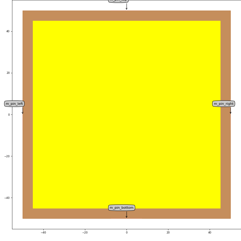
Bondpads
BondPad
Bond pad for the electrical probing
from siepic_shuksan import technology
from siepic_shuksan.all import BondPad
lo = BondPad().Layout()
lo.visualize(annotate=True, box=None, canvas_size=(1000.0, None))
Ports
Name |
Type |
Position |
Angle |
Waveguide Template |
Inclination |
|---|---|---|---|---|---|
m_pin_left |
Electrical |
(-50.0,0.0) |
180.0 |
M2WireTemplate |
0.0 |
m_pin_right |
Electrical |
(50.0,0.0) |
0.0 |
M2WireTemplate |
0.0 |
m_pin_bottom |
Electrical |
(0.0,-50.0) |
-90.0 |
M2WireTemplate |
0.0 |
m_pin_top |
Electrical |
(0.0,50.0) |
90.0 |
M2WireTemplate |
0.0 |
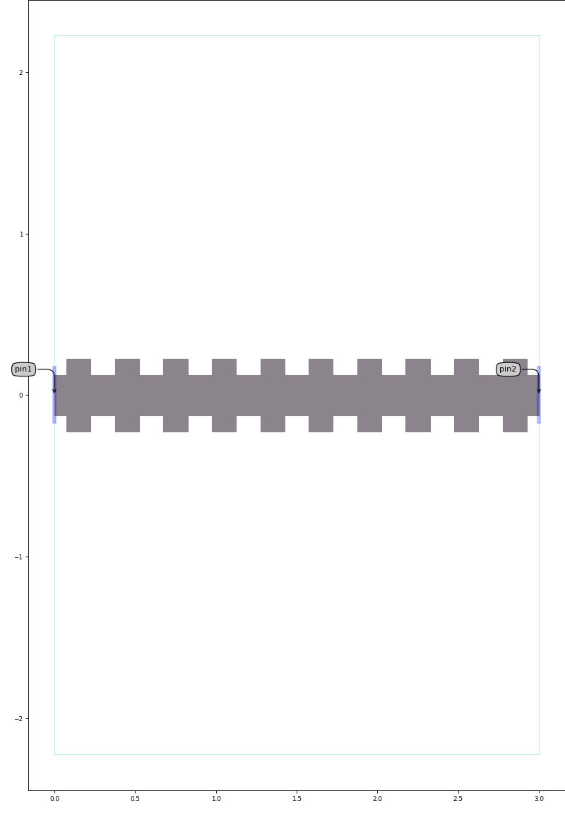
Directional Couplers
DirectionalCoupler
Directional coupler or evanescent coupler where the gap, bending radius and coupling length are user defined. This PCell does not have a circuit model.
- Parameters:
- radius: float and number > 0
Gap between the waveguides
- coupling_length: float and Real, number and number >= 0
Length of the coupling straight section
- gap: float and number > 0
Gap between the waveguides
- name: String that contains only ISO/IEC 8859-1 (extended ASCII py3) or pure ASCII (py2) characters
The unique name of the pcell
from siepic_shuksan import technology
from siepic_shuksan.all import DirectionalCoupler
lo = DirectionalCoupler().Layout()
lo.visualize(annotate=True, box=None, canvas_size=(1000.0, None))
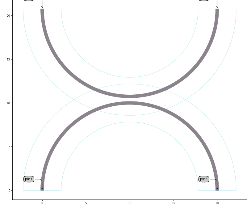
Ports
Name |
Type |
Position |
Angle |
Waveguide Template |
Inclination |
|---|---|---|---|---|---|
pin1 |
Optical |
(0.0,0.0) |
-90.0 |
WaveguideWireTemplate |
0.0 |
pin3 |
Optical |
(20.0,0.0) |
-90.0 |
WaveguideWireTemplate |
0.0 |
pin2 |
Optical |
(0.0,20.75) |
90.0 |
WaveguideWireTemplate |
0.0 |
pin4 |
Optical |
(20.0,20.75) |
90.0 |
WaveguideWireTemplate |
0.0 |
Layout
Parameters
- view_name: String that contains only alphanumeric characters from the ASCII set or contains _$. ASCII set is extended on PY3.
The name of the view
Electric Wires
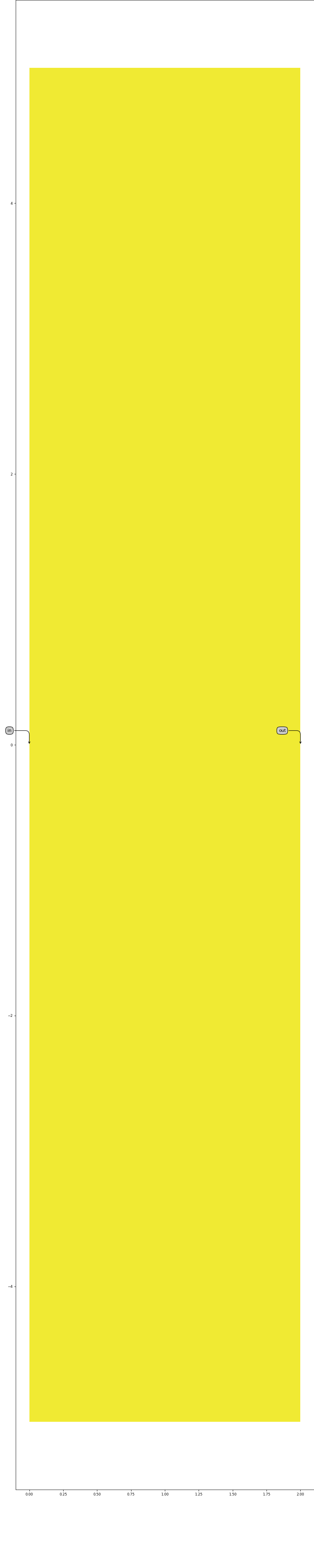
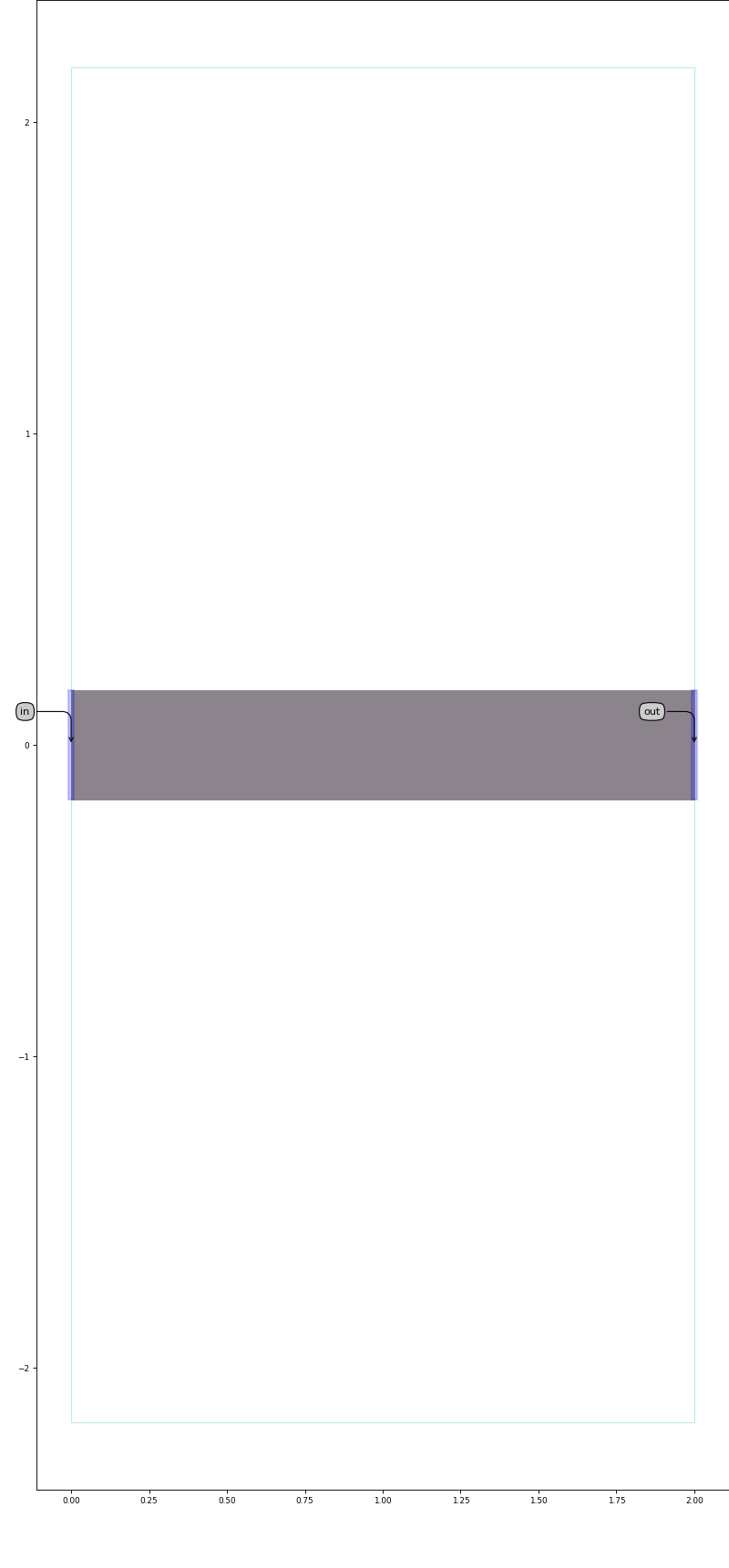
HeaterWire
Heater metal wire for creating heaters.
- Parameters:
- metal_width: float and number > 0
Width of the metal layer [um]
- trace_template: PCell and _WaveguideTemplate
- name: String that contains only ISO/IEC 8859-1 (extended ASCII py3) or pure ASCII (py2) characters
The unique name of the pcell
from siepic_shuksan import technology
from siepic_shuksan.all import HeaterWire
lo = HeaterWire().Layout()
lo.visualize(annotate=True, box=None, canvas_size=(1000.0, None))
Ports
Name |
Type |
Position |
Angle |
Waveguide Template |
Inclination |
|---|---|---|---|---|---|
in |
Optical |
(0.0,0.0) |
180.0 |
HeaterWireTemplate |
0.0 |
out |
Optical |
(2.0,0.0) |
0.0 |
HeaterWireTemplate |
0.0 |
Layout
Parameters
- shape: Shape
Shape from which the Trace is calculated
- bend_radius: float and number > 0
Bend radius for the auto-generated bends.
CircuitModel
Parameters
- length: float and Real, number and number >= 0
The physical length of the waveguide during simulation
layout_view: ( _LayoutView ), None allowed netlist_view: ( NetlistView ), None allowed view_name: String that contains only alphanumeric characters from the ASCII set or contains _$. ASCII set is extended on PY3.
The name of the view
Other Parameters
- solver: str and String that contains only ISO/IEC 8859-1 (extended ASCII py3) or pure ASCII (py2) characters, locked
circuit solver to use
M2Wire
DC metal wire defined in the M2 layer.
- Parameters:
- m_width: float and number > 0
Width of the metal routing [um]
- trace_template: PCell and ElectricalWireTemplate
- name: String that contains only ISO/IEC 8859-1 (extended ASCII py3) or pure ASCII (py2) characters
The unique name of the pcell
from siepic_shuksan import technology
from siepic_shuksan.all import M2Wire
lo = M2Wire().Layout()
lo.visualize(annotate=True, box=None, canvas_size=(1000.0, None))

Ports
Name |
Type |
Position |
Angle |
Waveguide Template |
Inclination |
|---|---|---|---|---|---|
in |
Electrical |
(0.0,0.0) |
180.0 |
M2WireTemplate |
0.0 |
out |
Electrical |
(50.0,-0.0) |
0.0 |
M2WireTemplate |
0.0 |
Layout
Parameters
- shape: Shape
Shape from which the Trace is calculated
CircuitModel
Parameters
layout_view: ( _LayoutView ), None allowed netlist_view: ( NetlistView ), None allowed view_name: String that contains only alphanumeric characters from the ASCII set or contains _$. ASCII set is extended on PY3.
The name of the view
Other Parameters
- solver: str and String that contains only ISO/IEC 8859-1 (extended ASCII py3) or pure ASCII (py2) characters, locked
circuit solver to use
Floor Plan
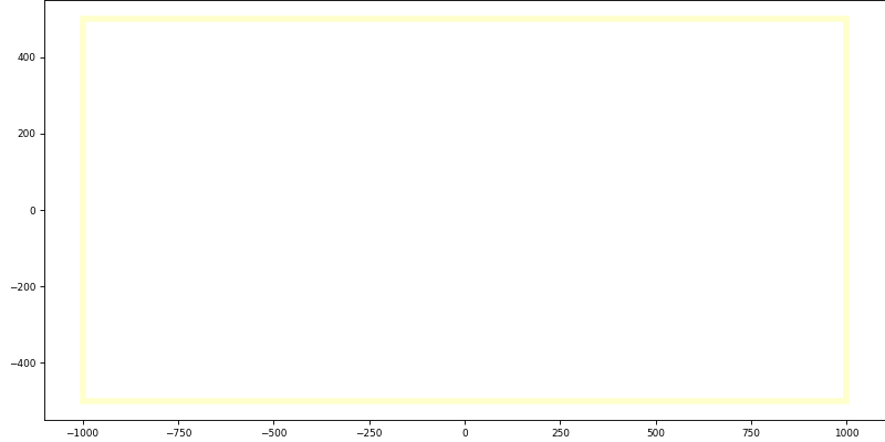
Floorplan
Chip floor plan on which the integrated designs are drawn.
- Parameters:
- height: float and number > 0
Height of the floorplan [mu]
- width: float and number > 0
Width of the floorplan [mu]
- name: String that contains only ISO/IEC 8859-1 (extended ASCII py3) or pure ASCII (py2) characters
The unique name of the pcell
from siepic_shuksan import technology
from siepic_shuksan.all import Floorplan
lo = Floorplan().Layout()
lo.visualize(annotate=True, box=None, canvas_size=(1000.0, None))
Layout
Parameters
- view_name: String that contains only alphanumeric characters from the ASCII set or contains _$. ASCII set is extended on PY3.
The name of the view
Grating couplers
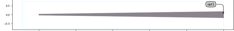
GC_1270_TE_8deg
Fiber grating coupler for operation at 1270 nm and TE polarization, under an angle of 8 degrees
from siepic_shuksan import technology
from siepic_shuksan.all import GC_1270_TE_8deg
lo = GC_1270_TE_8deg().Layout()
lo.visualize(annotate=True, box=None, canvas_size=(1000.0, None))

Ports
Name |
Type |
Position |
Angle |
Waveguide Template |
Inclination |
|---|---|---|---|---|---|
opt1 |
Optical |
(0.0,0.0) |
0.0 |
WaveguideWireTemplate |
0.0 |
fib1 |
Optical |
(-21.762,-0.069) |
8.0 |
0.0 |
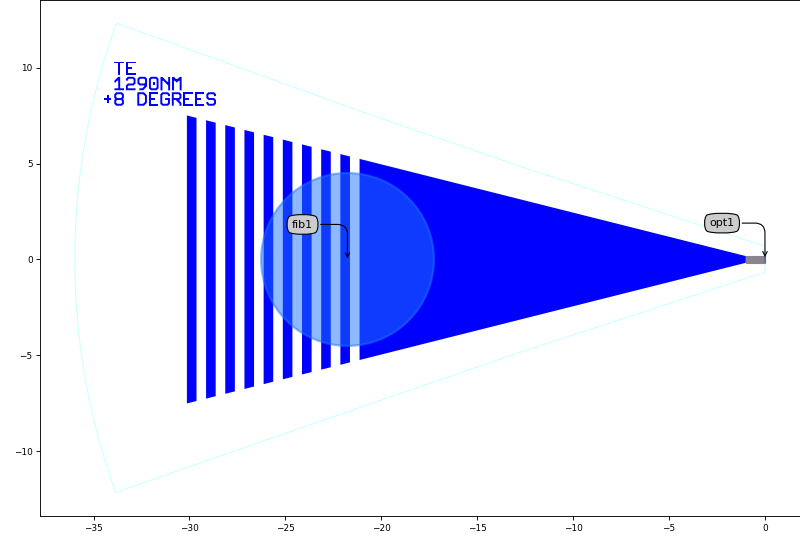
GC_1290_TE_8deg
Fiber grating coupler for operation at 1290 nm and TE polarization, under an angle of 8 degrees
from siepic_shuksan import technology
from siepic_shuksan.all import GC_1290_TE_8deg
lo = GC_1290_TE_8deg().Layout()
lo.visualize(annotate=True, box=None, canvas_size=(1000.0, None))
Ports
Name |
Type |
Position |
Angle |
Waveguide Template |
Inclination |
|---|---|---|---|---|---|
fib1 |
Optical |
(-21.762,-0.069) |
8.0 |
0.0 |
|
opt1 |
Optical |
(0.0,0.0) |
0.0 |
WaveguideWireTemplate |
0.0 |
GC_1310_TE_8deg
Fiber grating coupler for operation at 1310 nm and TE polarization, under an angle of 8 degrees
from siepic_shuksan import technology
from siepic_shuksan.all import GC_1310_TE_8deg
lo = GC_1310_TE_8deg().Layout()
lo.visualize(annotate=True, box=None, canvas_size=(1000.0, None))

Ports
Name |
Type |
Position |
Angle |
Waveguide Template |
Inclination |
|---|---|---|---|---|---|
fib1 |
Optical |
(-21.762,-0.069) |
8.0 |
0.0 |
|
opt1 |
Optical |
(0.0,0.0) |
0.0 |
WaveguideWireTemplate |
0.0 |
GC_1330_TE_8deg
Fiber grating coupler for operation at 1330 nm and TE polarization, under an angle of 8 degrees
from siepic_shuksan import technology
from siepic_shuksan.all import GC_1330_TE_8deg
lo = GC_1330_TE_8deg().Layout()
lo.visualize(annotate=True, box=None, canvas_size=(1000.0, None))

Ports
Name |
Type |
Position |
Angle |
Waveguide Template |
Inclination |
|---|---|---|---|---|---|
fib1 |
Optical |
(-21.762,-0.069) |
8.0 |
0.0 |
|
opt1 |
Optical |
(0.0,0.0) |
0.0 |
WaveguideWireTemplate |
0.0 |
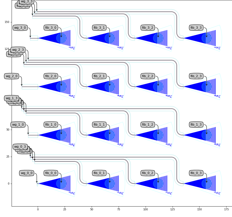
Grating Coupler Matrix
GratingCouplerMatrix
Fully parametric matrix of grating couplers, including parameters for placing the routing waveguides. Circuit model is derived from the hierarchical model.
- Parameters:
- add_extensions: ( bool, bool_ or int )
Adding extensions to the output waveguides for easier and more robust external routing
- wg_sep: float and number > 0
Separation between the waveguide
- wg_radius: float and number > 0
Radius of the routed waveguide bends
- wg_str_len: float and Real, number and number >= 0
Length straight wavelength at the GC port
- gc_sep_y: float and number > 0
Vertical separation between the grating couplers
- gc_sep_x: float and number > 0
Horizontal separation between the grating couplers
- gc: PCell
Grating coupler cell (only for 1D gratings)
- n_cols: int
Number of GC columns
- n_rows: int
Number of GC rows
- strict: ( bool, bool_ or int )
If True, any error will raise an exception and stop the program flow. If False, any routing error will give a warning and draw a straight line on an error layer. See
i3.ConnectLogicalfor more information.- exposed_ports: ( dict ), *None allowed*
Ports to be exposed, mapping {‘instance_name:port_name’: external_port_name’} map for i3.expose_ports().Set to None (default) to expose all unconnected ports
- specs: list
Placement and routing specifications
- insts: OrderedDict and key: str, value: PCell, _View
Instances of child cells which this circuit is composed of: {‘instance_name’: cell, …} where cell is an i3.PCell object.
- name: String that contains only ISO/IEC 8859-1 (extended ASCII py3) or pure ASCII (py2) characters
The unique name of the pcell
from siepic_shuksan import technology
from siepic_shuksan.all import GratingCouplerMatrix
lo = GratingCouplerMatrix().Layout()
lo.visualize(annotate=True, box=None, canvas_size=(1000.0, None))
Ports
Name |
Type |
Position |
Angle |
Waveguide Template |
Inclination |
|---|---|---|---|---|---|
fib_0_0 |
Optical |
(21.762,0.069) |
-172.0 |
0.0 |
|
wg_0_0 |
Optical |
(-1.0,0.0) |
180.0 |
WaveguideWireTemplate |
0.0 |
fib_0_1 |
Optical |
(66.762,0.069) |
-172.0 |
0.0 |
|
wg_0_1 |
Optical |
(-3.0,20.5) |
180.0 |
WaveguideWireTemplate |
0.0 |
fib_0_2 |
Optical |
(111.762,0.069) |
-172.0 |
0.0 |
|
wg_0_2 |
Optical |
(-5.0,22.5) |
180.0 |
WaveguideWireTemplate |
0.0 |
fib_0_3 |
Optical |
(156.762,0.069) |
-172.0 |
0.0 |
|
wg_0_3 |
Optical |
(-7.0,24.5) |
180.0 |
WaveguideWireTemplate |
0.0 |
fib_1_0 |
Optical |
(21.762,45.069) |
-172.0 |
0.0 |
|
wg_1_0 |
Optical |
(-9.0,45.0) |
180.0 |
WaveguideWireTemplate |
0.0 |
fib_1_1 |
Optical |
(66.762,45.069) |
-172.0 |
0.0 |
|
wg_1_1 |
Optical |
(-11.0,65.5) |
180.0 |
WaveguideWireTemplate |
0.0 |
fib_1_2 |
Optical |
(111.762,45.069) |
-172.0 |
0.0 |
|
wg_1_2 |
Optical |
(-13.0,67.5) |
180.0 |
WaveguideWireTemplate |
0.0 |
fib_1_3 |
Optical |
(156.762,45.069) |
-172.0 |
0.0 |
|
wg_1_3 |
Optical |
(-15.0,69.5) |
180.0 |
WaveguideWireTemplate |
0.0 |
fib_2_0 |
Optical |
(21.762,90.069) |
-172.0 |
0.0 |
|
wg_2_0 |
Optical |
(-15.0,90.0) |
180.0 |
WaveguideWireTemplate |
0.0 |
fib_2_1 |
Optical |
(66.762,90.069) |
-172.0 |
0.0 |
|
wg_2_1 |
Optical |
(-13.0,110.5) |
180.0 |
WaveguideWireTemplate |
0.0 |
fib_2_2 |
Optical |
(111.762,90.069) |
-172.0 |
0.0 |
|
wg_2_2 |
Optical |
(-11.0,112.5) |
180.0 |
WaveguideWireTemplate |
0.0 |
fib_2_3 |
Optical |
(156.762,90.069) |
-172.0 |
0.0 |
|
wg_2_3 |
Optical |
(-9.0,114.5) |
180.0 |
WaveguideWireTemplate |
0.0 |
fib_3_0 |
Optical |
(21.762,135.069) |
-172.0 |
0.0 |
|
wg_3_0 |
Optical |
(-7.0,135.0) |
180.0 |
WaveguideWireTemplate |
0.0 |
fib_3_1 |
Optical |
(66.762,135.069) |
-172.0 |
0.0 |
|
wg_3_1 |
Optical |
(-5.0,155.5) |
180.0 |
WaveguideWireTemplate |
0.0 |
fib_3_2 |
Optical |
(111.762,135.069) |
-172.0 |
0.0 |
|
wg_3_2 |
Optical |
(-3.0,157.5) |
180.0 |
WaveguideWireTemplate |
0.0 |
fib_3_3 |
Optical |
(156.762,135.069) |
-172.0 |
0.0 |
|
wg_3_3 |
Optical |
(-1.0,159.5) |
180.0 |
WaveguideWireTemplate |
0.0 |
Layout
Parameters
- view_name: String that contains only alphanumeric characters from the ASCII set or contains _$. ASCII set is extended on PY3.
The name of the view
CircuitModel
Parameters
layout_view: ( _LayoutView ), None allowed netlist_view: ( NetlistView ), None allowed view_name: String that contains only alphanumeric characters from the ASCII set or contains _$. ASCII set is extended on PY3.
The name of the view
Other Parameters
- solver: str and String that contains only ISO/IEC 8859-1 (extended ASCII py3) or pure ASCII (py2) characters, locked
circuit solver to use
Heaters
wg_heater
The wg_heater is a thermo-optic device that performs as a phase shifter. The heater length and width are 200 micron and 4 micron, respectively.
from siepic_shuksan import technology
from siepic_shuksan.all import wg_heater
lo = wg_heater().Layout()
lo.visualize(annotate=True, box=None, canvas_size=(1000.0, None))

Ports
Name |
Type |
Position |
Angle |
Waveguide Template |
Inclination |
|---|---|---|---|---|---|
opt1 |
Optical |
(0.0,0.0) |
180.0 |
WaveguideWireTemplate |
0.0 |
opt2 |
Optical |
(200.0,0.0) |
0.0 |
WaveguideWireTemplate |
0.0 |
m_pin1 |
Optical |
(10.0,2.0) |
90.0 |
WaveguideWireTemplate |
0.0 |
m_pin2 |
Optical |
(190.0,2.0) |
90.0 |
WaveguideWireTemplate |
0.0 |
Lasers
laser_1270nm
Laser black box emitting light at 1270 nm
from siepic_shuksan import technology
from siepic_shuksan.all import laser_1270nm
lo = laser_1270nm().Layout()
lo.visualize(annotate=True, box=None, canvas_size=(1000.0, None))

Ports
Name |
Type |
Position |
Angle |
Waveguide Template |
Inclination |
|---|---|---|---|---|---|
opt1 |
Optical |
(0.0,0.0) |
0.0 |
WaveguideWireTemplate |
0.0 |
elec1_p |
Electrical |
(-900.0,-149.63) |
180.0 |
M2WireTemplate |
0.0 |
elec2_n |
Electrical |
(-900.0,100.37) |
180.0 |
M2WireTemplate |
0.0 |
laser_1290nm
Laser black box emitting light at 1290 nm
from siepic_shuksan import technology
from siepic_shuksan.all import laser_1290nm
lo = laser_1290nm().Layout()
lo.visualize(annotate=True, box=None, canvas_size=(1000.0, None))

Ports
Name |
Type |
Position |
Angle |
Waveguide Template |
Inclination |
|---|---|---|---|---|---|
opt1 |
Optical |
(0.0,0.0) |
0.0 |
WaveguideWireTemplate |
0.0 |
elec1_p |
Electrical |
(-900.0,-149.63) |
180.0 |
M2WireTemplate |
0.0 |
elec2_n |
Electrical |
(-900.0,100.37) |
180.0 |
M2WireTemplate |
0.0 |
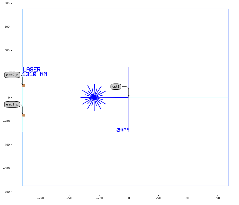
laser_1310nm
Laser black box emitting light at 1310 nm
from siepic_shuksan import technology
from siepic_shuksan.all import laser_1310nm
lo = laser_1310nm().Layout()
lo.visualize(annotate=True, box=None, canvas_size=(1000.0, None))
Ports
Name |
Type |
Position |
Angle |
Waveguide Template |
Inclination |
|---|---|---|---|---|---|
opt1 |
Optical |
(0.0,0.0) |
0.0 |
WaveguideWireTemplate |
0.0 |
elec1_p |
Electrical |
(-900.0,-149.63) |
180.0 |
M2WireTemplate |
0.0 |
elec2_n |
Electrical |
(-900.0,100.37) |
180.0 |
M2WireTemplate |
0.0 |
laser_1330nm
Laser black box emitting light at 1330 nm
from siepic_shuksan import technology
from siepic_shuksan.all import laser_1330nm
lo = laser_1330nm().Layout()
lo.visualize(annotate=True, box=None, canvas_size=(1000.0, None))

Ports
Name |
Type |
Position |
Angle |
Waveguide Template |
Inclination |
|---|---|---|---|---|---|
opt1 |
Optical |
(0.0,0.0) |
0.0 |
WaveguideWireTemplate |
0.0 |
elec1_p |
Electrical |
(-900.0,-149.63) |
180.0 |
M2WireTemplate |
0.0 |
elec2_n |
Electrical |
(-900.0,100.37) |
180.0 |
M2WireTemplate |
0.0 |
Photonic Wire Bonds
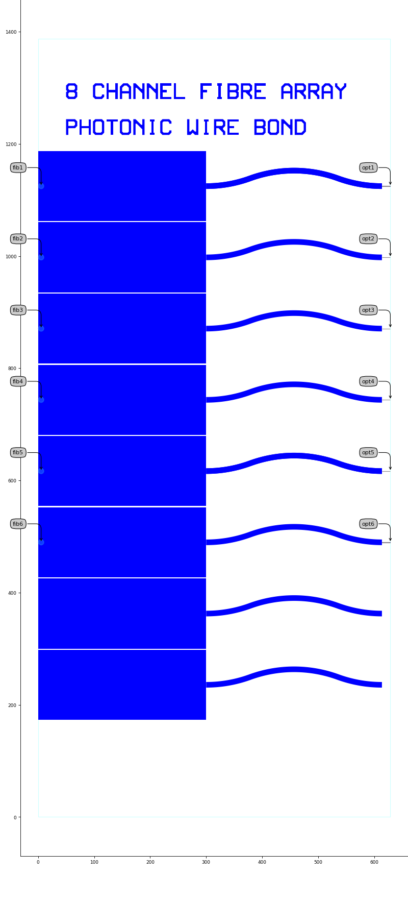
pwb_8ch_array
8 photonic wire bonds for optical fibre array coupling
from siepic_shuksan import technology
from siepic_shuksan.all import pwb_8ch_array
lo = pwb_8ch_array().Layout()
lo.visualize(annotate=True, box=None, canvas_size=(1000.0, None))
Ports
Name |
Type |
Position |
Angle |
Waveguide Template |
Inclination |
|---|---|---|---|---|---|
opt6 |
Optical |
(628.6,489.7) |
0.0 |
WaveguideWireTemplate |
0.0 |
opt5 |
Optical |
(628.6,616.7) |
0.0 |
WaveguideWireTemplate |
0.0 |
opt4 |
Optical |
(628.6,743.7) |
0.0 |
WaveguideWireTemplate |
0.0 |
opt3 |
Optical |
(628.6,870.7) |
0.0 |
WaveguideWireTemplate |
0.0 |
opt2 |
Optical |
(628.6,997.7) |
0.0 |
WaveguideWireTemplate |
0.0 |
opt1 |
Optical |
(628.6,1124.7) |
0.0 |
WaveguideWireTemplate |
0.0 |
fib6 |
Optical |
(5.527,489.649) |
8.0 |
0.0 |
|
fib5 |
Optical |
(5.527,616.649) |
8.0 |
0.0 |
|
fib4 |
Optical |
(5.527,743.649) |
8.0 |
0.0 |
|
fib3 |
Optical |
(5.527,870.649) |
8.0 |
0.0 |
|
fib2 |
Optical |
(5.527,997.649) |
8.0 |
0.0 |
|
fib1 |
Optical |
(5.527,1124.649) |
8.0 |
0.0 |
Ring Based Components
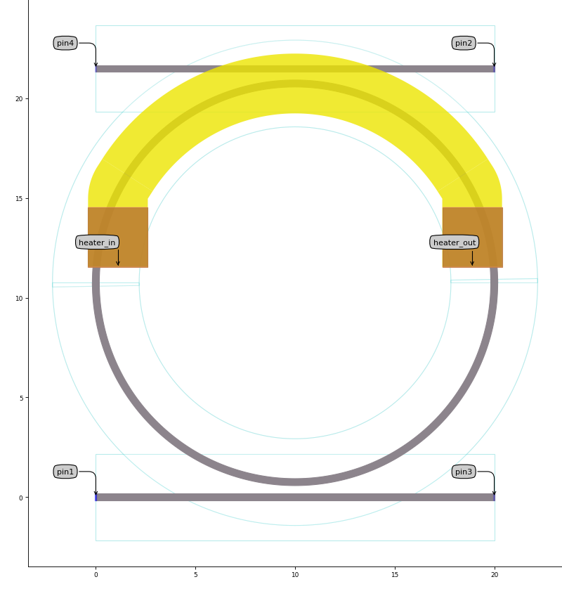
RingFilterTunableGeneral
Heated add-drop ring/racetrack where the gaps, bending radius, coupling length, heater length, width and contact length are user defined. Also the widths of the ring waveguide and adjacent waveguides can all be set independently. This PCell does not have a circuit model.
- Parameters:
- heater_contact_length: float and Real, number and number >= 0
Length of the heater contact
- heater_width: float and Real, number and number >= 0
Length of the heater length
- heater_length: float and Real, number and number >= 0
Length of the heater length
- coupling_length: float and Real, number and number >= 0
Length of the coupling straight section
- wg_top_width: float and number > 0
Width of the top adjacent waveguide
- wg_ring_width: float and number > 0
Width of the ring waveguide
- wg_bot_width: float and number > 0
Width of the bottom adjacent waveguide
- radius: float and number > 0
Gap between the waveguides
- gap_top: float and number > 0
Gap between the waveguides
- gap_bot: float and number > 0
Gap between the waveguides
- name: String that contains only ISO/IEC 8859-1 (extended ASCII py3) or pure ASCII (py2) characters
The unique name of the pcell
from siepic_shuksan import technology
from siepic_shuksan.all import RingFilterTunableGeneral
lo = RingFilterTunableGeneral().Layout()
lo.visualize(annotate=True, box=None, canvas_size=(1000.0, None))
Ports
Name |
Type |
Position |
Angle |
Waveguide Template |
Inclination |
|---|---|---|---|---|---|
pin1 |
Optical |
(0.0,0.0) |
180.0 |
WaveguideWireTemplate |
0.0 |
pin3 |
Optical |
(20.0,0.0) |
0.0 |
WaveguideWireTemplate |
0.0 |
pin4 |
Optical |
(0.0,21.5) |
180.0 |
WaveguideWireTemplate |
0.0 |
pin2 |
Optical |
(20.0,21.5) |
0.0 |
WaveguideWireTemplate |
0.0 |
heater_in |
Electrical |
(1.11,11.532) |
-90.0 |
M2WireTemplate |
0.0 |
heater_out |
Electrical |
(18.89,11.532) |
-90.0 |
M2WireTemplate |
0.0 |
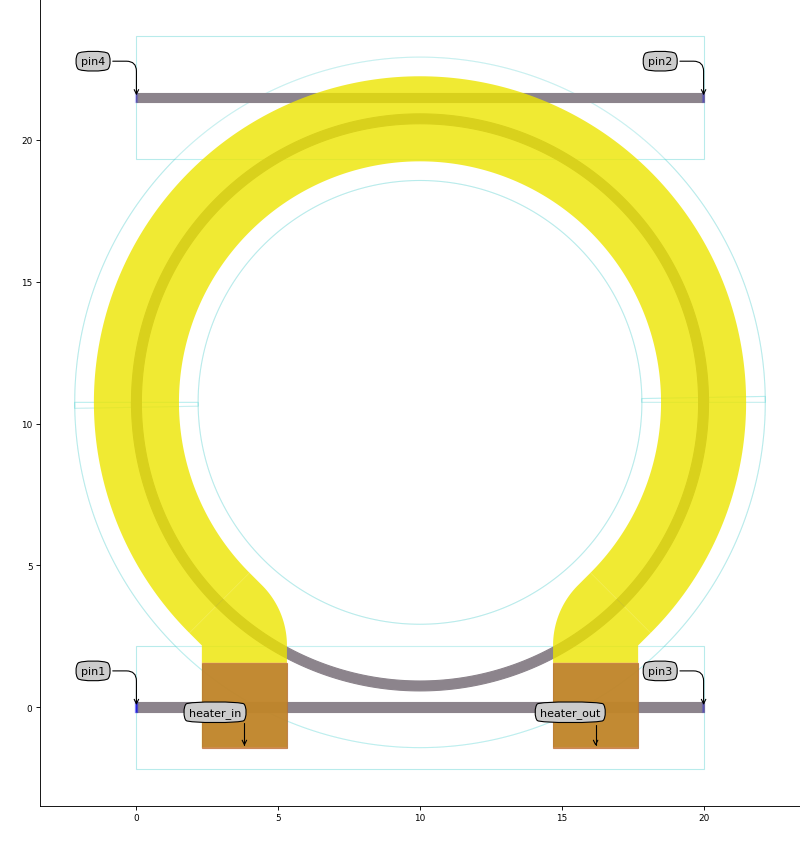
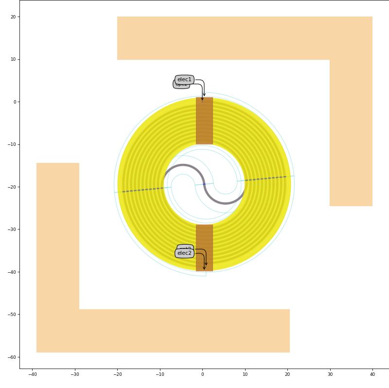
RingFilterTunable
Heated add-drop ring/racetrack where the gaps, bending radius, coupling length, waveguide width and heater width are user defined. This PCell does not have a circuit model.
- Parameters:
- wg_width: float and number > 0
Width of the waveguides
- heater_width: float and Real, number and number >= 0
Length of the heater length
- coupling_length: float and Real, number and number >= 0
Length of the coupling straight section
- radius: float and number > 0
Gap between the waveguides
- gap_top: float and number > 0
Gap between the waveguides
- gap_bot: float and number > 0
Gap between the waveguides
- name: String that contains only ISO/IEC 8859-1 (extended ASCII py3) or pure ASCII (py2) characters
The unique name of the pcell
from siepic_shuksan import technology
from siepic_shuksan.all import RingFilterTunable
lo = RingFilterTunable().Layout()
lo.visualize(annotate=True, box=None, canvas_size=(1000.0, None))
Ports
Name |
Type |
Position |
Angle |
Waveguide Template |
Inclination |
|---|---|---|---|---|---|
pin1 |
Optical |
(0.0,0.0) |
180.0 |
WaveguideWireTemplate |
0.0 |
pin3 |
Optical |
(20.0,0.0) |
0.0 |
WaveguideWireTemplate |
0.0 |
pin4 |
Optical |
(0.0,21.5) |
180.0 |
WaveguideWireTemplate |
0.0 |
pin2 |
Optical |
(20.0,21.5) |
0.0 |
WaveguideWireTemplate |
0.0 |
heater_in |
Electrical |
(3.808,-1.442) |
-90.0 |
M2WireTemplate |
0.0 |
heater_out |
Electrical |
(16.192,-1.442) |
-90.0 |
M2WireTemplate |
0.0 |
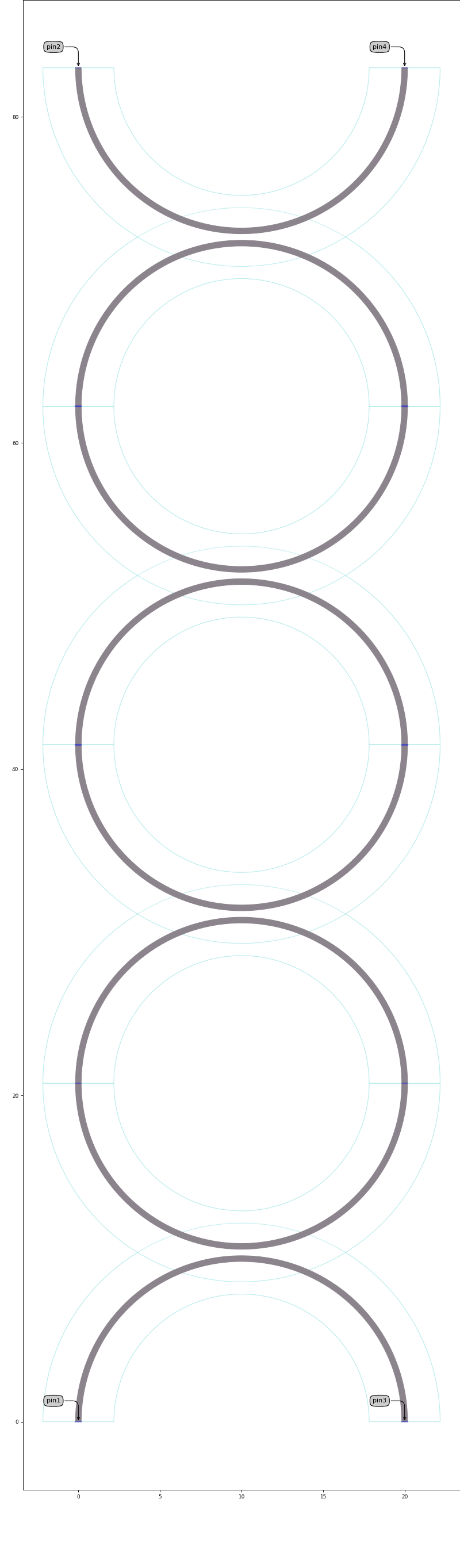
SeriesRings
Rings/racetracks evanescently coupled in series where the gap, bending radius, coupling length and number of rings are user defined. This PCell does not have a circuit model.
- Parameters:
- num_rings: int
Number of rings
- radius: float and number > 0
Gap between the waveguides
- coupling_length: float and Real, number and number >= 0
Length of the coupling straight section
- gap: float and number > 0
Gap between the waveguides
- name: String that contains only ISO/IEC 8859-1 (extended ASCII py3) or pure ASCII (py2) characters
The unique name of the pcell
from siepic_shuksan import technology
from siepic_shuksan.all import SeriesRings
lo = SeriesRings().Layout()
lo.visualize(annotate=True, box=None, canvas_size=(1000.0, None))
Ports
Name |
Type |
Position |
Angle |
Waveguide Template |
Inclination |
|---|---|---|---|---|---|
pin1 |
Optical |
(0.0,0.0) |
-90.0 |
WaveguideWireTemplate |
0.0 |
pin3 |
Optical |
(20.0,0.0) |
-90.0 |
WaveguideWireTemplate |
0.0 |
pin2 |
Optical |
(0.0,83.0) |
90.0 |
WaveguideWireTemplate |
0.0 |
pin4 |
Optical |
(20.0,83.0) |
90.0 |
WaveguideWireTemplate |
0.0 |
Layout
Parameters
- view_name: String that contains only alphanumeric characters from the ASCII set or contains _$. ASCII set is extended on PY3.
The name of the view
Spirals
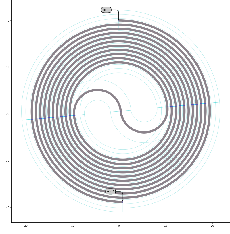
SpiralCircular
Circular spiral with a fixed length. The angular offset to achieve a given spiral length, with a given set of parameters such as the radius of the central bends, the spacing between the waveguides and the core width, is automatically calculated. This PCell does not contain heaters and is thus purely used for delay.
- Parameters:
- spiral_length: float and number > 0
Length of the total spiral waveguide
- spacing: float and number > 0
Separation between adjacent waveguides
- radius: float and number > 0
Radius of the central bends
- core_width: float and number > 0
Core width of the bend waveguide
- name: String that contains only ISO/IEC 8859-1 (extended ASCII py3) or pure ASCII (py2) characters
The unique name of the pcell
- Other Parameters:
- layout_properties: ndarray, locked
Calculated layout properties of the spiral.
from siepic_shuksan import technology
from siepic_shuksan.all import SpiralCircular
lo = SpiralCircular().Layout()
lo.visualize(annotate=True, box=None, canvas_size=(1000.0, None))
Ports
Name |
Type |
Position |
Angle |
Waveguide Template |
Inclination |
|---|---|---|---|---|---|
opt1 |
Optical |
(0.0,0.0) |
180.0 |
WaveguideWireTemplate |
0.0 |
opt2 |
Optical |
(0.896,-38.817) |
0.0 |
WaveguideWireTemplate |
0.0 |
Layout
Parameters
- view_name: String that contains only alphanumeric characters from the ASCII set or contains _$. ASCII set is extended on PY3.
The name of the view
CircuitModel
Parameters
- vbias: float
Heater bias voltage (use only for frequency domain simulations) [V]
- optical_correction_factor: float and Real, number and number >= 0
Correction factor taking into account how much optical waveguide is below the heater. It is calculated as being the length of the optical waveguide below the heater divided by the heater length.
- resistance: float and number > 0
Resistance of the heater material [Ohm]
- resistivity: float and number > 0
Resistivity of the heater material [Ohm]
- p_pi: float and number > 0
Power needed for a pi phase shift on the full heater [W]
- length: float and number > 0
Length of the trace [micron]
- loss_db_per_cm: float and number > 0
Waveguide propagation loss [dB/cm]
- wavelength_bounds: ndarray
Wavelength range in which the model is valid
- ng_fit_coeff: ndarray
Fit coefficients of the group indices
- neff_fit_coeff: ndarray
Fit coefficients of the effective indices
layout_view: ( _LayoutView ), None allowed netlist_view: ( NetlistView ), None allowed view_name: String that contains only alphanumeric characters from the ASCII set or contains _$. ASCII set is extended on PY3.
The name of the view
Other Parameters
- solver: str and String that contains only ISO/IEC 8859-1 (extended ASCII py3) or pure ASCII (py2) characters, locked
circuit solver to use
SpiralCircularWithHeater
Circular spiral with a fixed length, covered with a circular heater. The angular offset to achieve a given spiral length, with a given set of parameters such as the radius of the central bends, the spacing between the waveguides and the core width, is automatically calculated. The angular position of the two contact pads on the heater can be changed but by default overlap with the input/output optical waveguides.
- Parameters:
- ox_open_xy_ext: Coord2
Open oxide region horizontal and vertical extension compared to the spiral center
- ox_open_sep: float and Real, number and number >= 0
Open oxide region separation from the spiral
- ox_open_width: float and Real, number and number >= 0
Width of open oxide region
- heater_width_extra: float
Width extension of the heater waveguide as compared to the inner and outer waveguide
- contacts_width: float and Real, number and number >= 0
Width of the contacts.
- contacts_angle: float
Angle of the contacts as compared with the input port
- spiral_length: float and number > 0
Length of the total spiral waveguide
- spacing: float and number > 0
Separation between adjacent waveguides
- radius: float and number > 0
Radius of the central bends
- core_width: float and number > 0
Core width of the bend waveguide
- name: String that contains only ISO/IEC 8859-1 (extended ASCII py3) or pure ASCII (py2) characters
The unique name of the pcell
- Other Parameters:
- layout_properties: ndarray, locked
Calculated layout properties of the spiral.
from siepic_shuksan import technology
from siepic_shuksan.all import SpiralCircularWithHeater
lo = SpiralCircularWithHeater().Layout()
lo.visualize(annotate=True, box=None, canvas_size=(1000.0, None))
Ports
Name |
Type |
Position |
Angle |
Waveguide Template |
Inclination |
|---|---|---|---|---|---|
opt1 |
Optical |
(0.0,0.0) |
180.0 |
WaveguideWireTemplate |
0.0 |
opt2 |
Optical |
(0.896,-38.817) |
0.0 |
WaveguideWireTemplate |
0.0 |
elec1 |
Electrical |
(0.448,0.991) |
90.0 |
M2WireTemplate |
0.0 |
elec2 |
Electrical |
(0.448,-39.809) |
-90.0 |
M2WireTemplate |
0.0 |
Layout
Parameters
- view_name: String that contains only alphanumeric characters from the ASCII set or contains _$. ASCII set is extended on PY3.
The name of the view
CircuitModel
Parameters
- vbias: float
Heater bias voltage (use only for frequency domain simulations) [V]
- optical_correction_factor: float and Real, number and number >= 0
Correction factor taking into account how much optical waveguide is below the heater. It is calculated as being the length of the optical waveguide below the heater divided by the heater length.
- resistance: float and number > 0
Resistance of the heater material [Ohm]
- resistivity: float and number > 0
Resistivity of the heater material [Ohm]
- p_pi: float and number > 0
Power needed for a pi phase shift on the full heater [W]
- length: float and number > 0
Length of the trace [micron]
- loss_db_per_cm: float and number > 0
Waveguide propagation loss [dB/cm]
- wavelength_bounds: ndarray
Wavelength range in which the model is valid
- ng_fit_coeff: ndarray
Fit coefficients of the group indices
- neff_fit_coeff: ndarray
Fit coefficients of the effective indices
layout_view: ( _LayoutView ), None allowed netlist_view: ( NetlistView ), None allowed view_name: String that contains only alphanumeric characters from the ASCII set or contains _$. ASCII set is extended on PY3.
The name of the view
Other Parameters
- solver: str and String that contains only ISO/IEC 8859-1 (extended ASCII py3) or pure ASCII (py2) characters, locked
circuit solver to use
Heated Spiral Matrix
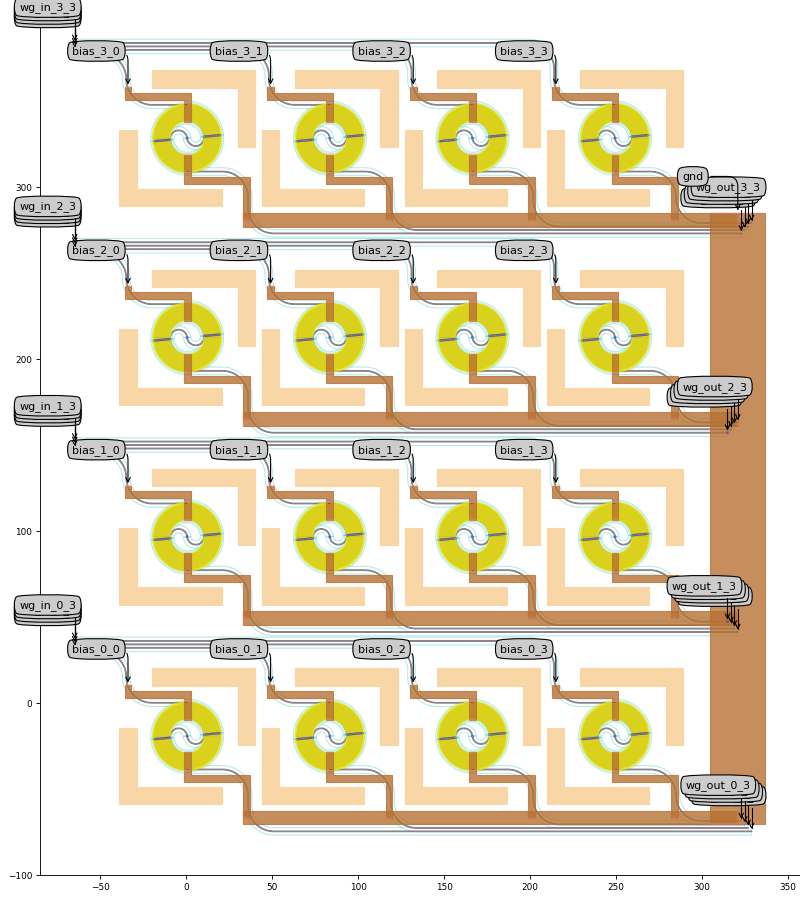
HeatedSpiralMatrix
Fully parametric matrix of heated spiral, including parameters for placing the routing waveguides and electric wires. Circuit model is derived from the hierarchical model, with the netlist being adapted in order to enable circuit simulations.
- Parameters:
- add_extensions: ( bool, bool_ or int )
Adding extensions to the output waveguides for easier and more robust external routing
- add_common_ground: ( bool, bool_ or int )
Create common ground for all the spirals
- wg_sep: float and number > 0
Separation between the waveguides
- wg_radius: float and number > 0
Radius of the routed waveguide bends
- wg_str_len: float and Real, number and number >= 0
Length straight wavelength at the spiral port and outputs
- spiral_sep_y: float and number > 0
Vertical separation between the spirals
- spiral_sep_x: float and number > 0
Horizontal separation between the spirals
- spiral: PCell
Spiral cell
- n_cols: int
Number of spiral columns
- n_rows: int
Number of spiral rows
- strict: ( bool, bool_ or int )
If True, any error will raise an exception and stop the program flow. If False, any routing error will give a warning and draw a straight line on an error layer. See
i3.ConnectLogicalfor more information.- exposed_ports: ( dict ), *None allowed*
Ports to be exposed, mapping {‘instance_name:port_name’: external_port_name’} map for i3.expose_ports().Set to None (default) to expose all unconnected ports
- specs: list
Placement and routing specifications
- insts: OrderedDict and key: str, value: PCell, _View
Instances of child cells which this circuit is composed of: {‘instance_name’: cell, …} where cell is an i3.PCell object.
- name: String that contains only ISO/IEC 8859-1 (extended ASCII py3) or pure ASCII (py2) characters
The unique name of the pcell
from siepic_shuksan import technology
from siepic_shuksan.all import HeatedSpiralMatrix
lo = HeatedSpiralMatrix().Layout()
lo.visualize(annotate=True, box=None, canvas_size=(1000.0, None))
Ports
Name |
Type |
Position |
Angle |
Waveguide Template |
Inclination |
|---|---|---|---|---|---|
wg_in_0_0 |
Optical |
(-65.0,30.0) |
180.0 |
WaveguideWireTemplate |
0.0 |
wg_out_0_0 |
Optical |
(328.896,-74.817) |
0.0 |
WaveguideWireTemplate |
0.0 |
bias_0_0 |
Electrical |
(-34.002,10.45) |
90.0 |
M2WireTemplate |
0.0 |
wg_in_0_1 |
Optical |
(-65.0,32.0) |
180.0 |
WaveguideWireTemplate |
0.0 |
wg_out_0_1 |
Optical |
(326.896,-72.817) |
0.0 |
WaveguideWireTemplate |
0.0 |
bias_0_1 |
Electrical |
(48.998,10.45) |
90.0 |
M2WireTemplate |
0.0 |
wg_in_0_2 |
Optical |
(-65.0,34.0) |
180.0 |
WaveguideWireTemplate |
0.0 |
wg_out_0_2 |
Optical |
(324.896,-70.817) |
0.0 |
WaveguideWireTemplate |
0.0 |
bias_0_2 |
Electrical |
(131.998,10.45) |
90.0 |
M2WireTemplate |
0.0 |
wg_in_0_3 |
Optical |
(-65.0,36.0) |
180.0 |
WaveguideWireTemplate |
0.0 |
wg_out_0_3 |
Optical |
(322.896,-68.817) |
0.0 |
WaveguideWireTemplate |
0.0 |
bias_0_3 |
Electrical |
(214.998,10.45) |
90.0 |
M2WireTemplate |
0.0 |
wg_in_1_0 |
Optical |
(-65.0,146.0) |
180.0 |
WaveguideWireTemplate |
0.0 |
wg_out_1_0 |
Optical |
(320.896,41.183) |
0.0 |
WaveguideWireTemplate |
0.0 |
bias_1_0 |
Electrical |
(-34.002,126.45) |
90.0 |
M2WireTemplate |
0.0 |
wg_in_1_1 |
Optical |
(-65.0,148.0) |
180.0 |
WaveguideWireTemplate |
0.0 |
wg_out_1_1 |
Optical |
(318.896,43.183) |
0.0 |
WaveguideWireTemplate |
0.0 |
bias_1_1 |
Electrical |
(48.998,126.45) |
90.0 |
M2WireTemplate |
0.0 |
wg_in_1_2 |
Optical |
(-65.0,150.0) |
180.0 |
WaveguideWireTemplate |
0.0 |
wg_out_1_2 |
Optical |
(316.896,45.183) |
0.0 |
WaveguideWireTemplate |
0.0 |
bias_1_2 |
Electrical |
(131.998,126.45) |
90.0 |
M2WireTemplate |
0.0 |
wg_in_1_3 |
Optical |
(-65.0,152.0) |
180.0 |
WaveguideWireTemplate |
0.0 |
wg_out_1_3 |
Optical |
(314.896,47.183) |
0.0 |
WaveguideWireTemplate |
0.0 |
bias_1_3 |
Electrical |
(214.998,126.45) |
90.0 |
M2WireTemplate |
0.0 |
wg_in_2_0 |
Optical |
(-65.0,262.0) |
180.0 |
WaveguideWireTemplate |
0.0 |
wg_out_2_0 |
Optical |
(314.896,157.183) |
0.0 |
WaveguideWireTemplate |
0.0 |
bias_2_0 |
Electrical |
(-34.002,242.45) |
90.0 |
M2WireTemplate |
0.0 |
wg_in_2_1 |
Optical |
(-65.0,264.0) |
180.0 |
WaveguideWireTemplate |
0.0 |
wg_out_2_1 |
Optical |
(316.896,159.183) |
0.0 |
WaveguideWireTemplate |
0.0 |
bias_2_1 |
Electrical |
(48.998,242.45) |
90.0 |
M2WireTemplate |
0.0 |
wg_in_2_2 |
Optical |
(-65.0,266.0) |
180.0 |
WaveguideWireTemplate |
0.0 |
wg_out_2_2 |
Optical |
(318.896,161.183) |
0.0 |
WaveguideWireTemplate |
0.0 |
bias_2_2 |
Electrical |
(131.998,242.45) |
90.0 |
M2WireTemplate |
0.0 |
wg_in_2_3 |
Optical |
(-65.0,268.0) |
180.0 |
WaveguideWireTemplate |
0.0 |
wg_out_2_3 |
Optical |
(320.896,163.183) |
0.0 |
WaveguideWireTemplate |
0.0 |
bias_2_3 |
Electrical |
(214.998,242.45) |
90.0 |
M2WireTemplate |
0.0 |
wg_in_3_0 |
Optical |
(-65.0,378.0) |
180.0 |
WaveguideWireTemplate |
0.0 |
wg_out_3_0 |
Optical |
(322.896,273.183) |
0.0 |
WaveguideWireTemplate |
0.0 |
bias_3_0 |
Electrical |
(-34.002,358.45) |
90.0 |
M2WireTemplate |
0.0 |
wg_in_3_1 |
Optical |
(-65.0,380.0) |
180.0 |
WaveguideWireTemplate |
0.0 |
wg_out_3_1 |
Optical |
(324.896,275.183) |
0.0 |
WaveguideWireTemplate |
0.0 |
bias_3_1 |
Electrical |
(48.998,358.45) |
90.0 |
M2WireTemplate |
0.0 |
wg_in_3_2 |
Optical |
(-65.0,382.0) |
180.0 |
WaveguideWireTemplate |
0.0 |
wg_out_3_2 |
Optical |
(326.896,277.183) |
0.0 |
WaveguideWireTemplate |
0.0 |
bias_3_2 |
Electrical |
(131.998,358.45) |
90.0 |
M2WireTemplate |
0.0 |
wg_in_3_3 |
Optical |
(-65.0,384.0) |
180.0 |
WaveguideWireTemplate |
0.0 |
wg_out_3_3 |
Optical |
(328.896,279.183) |
0.0 |
WaveguideWireTemplate |
0.0 |
bias_3_3 |
Electrical |
(214.998,358.45) |
90.0 |
M2WireTemplate |
0.0 |
gnd |
Electrical |
(320.898,285.183) |
90.0 |
M2WireTemplate |
0.0 |
Layout
Parameters
- view_name: String that contains only alphanumeric characters from the ASCII set or contains _$. ASCII set is extended on PY3.
The name of the view
CircuitModel
Parameters
layout_view: ( _LayoutView ), None allowed netlist_view: ( NetlistView ), None allowed view_name: String that contains only alphanumeric characters from the ASCII set or contains _$. ASCII set is extended on PY3.
The name of the view
Other Parameters
- solver: str and String that contains only ISO/IEC 8859-1 (extended ASCII py3) or pure ASCII (py2) characters, locked
circuit solver to use
Splitters
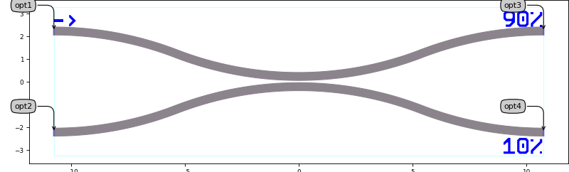
splitter_2x2_1310
2x2 splitter operating at TE and 1310 nm
from siepic_shuksan import technology
from siepic_shuksan.all import splitter_2x2_1310
lo = splitter_2x2_1310().Layout()
lo.visualize(annotate=True, box=None, canvas_size=(1000.0, None))

Ports
Name |
Type |
Position |
Angle |
Waveguide Template |
Inclination |
|---|---|---|---|---|---|
opt4 |
Optical |
(63.001,-2.0) |
0.0 |
WaveguideWireTemplate |
0.0 |
opt3 |
Optical |
(63.001,2.0) |
0.0 |
WaveguideWireTemplate |
0.0 |
opt2 |
Optical |
(-63.001,-2.0) |
180.0 |
WaveguideWireTemplate |
0.0 |
opt1 |
Optical |
(-63.001,2.0) |
180.0 |
WaveguideWireTemplate |
0.0 |
y_splitter_1310
1x2 Y-splitter operating at TE and 1310 nm
from siepic_shuksan import technology
from siepic_shuksan.all import y_splitter_1310
lo = y_splitter_1310().Layout()
lo.visualize(annotate=True, box=None, canvas_size=(1000.0, None))

Ports
Name |
Type |
Position |
Angle |
Waveguide Template |
Inclination |
|---|---|---|---|---|---|
opt1 |
Optical |
(0.0,0.0) |
180.0 |
WaveguideWireTemplate |
0.0 |
opt2 |
Optical |
(29.791,0.675) |
0.0 |
WaveguideWireTemplate |
0.0 |
opt3 |
Optical |
(29.791,-0.675) |
0.0 |
WaveguideWireTemplate |
0.0 |
tap_10_90_1270nm
This component is used to tap 10% of the input signal at 1270 nm. It can be also used at longer wavelengths, however, the power tapped will be slightly more than 10%.
from siepic_shuksan import technology
from siepic_shuksan.all import tap_10_90_1270nm
lo = tap_10_90_1270nm().Layout()
lo.visualize(annotate=True, box=None, canvas_size=(1000.0, None))
Ports
Name |
Type |
Position |
Angle |
Waveguide Template |
Inclination |
|---|---|---|---|---|---|
opt3 |
Optical |
(10.77,2.225) |
0.0 |
WaveguideWireTemplate |
0.0 |
opt4 |
Optical |
(10.77,-2.225) |
0.0 |
WaveguideWireTemplate |
0.0 |
opt2 |
Optical |
(-10.77,-2.225) |
180.0 |
WaveguideWireTemplate |
0.0 |
opt1 |
Optical |
(-10.77,2.225) |
180.0 |
WaveguideWireTemplate |
0.0 |
Splitter Trees
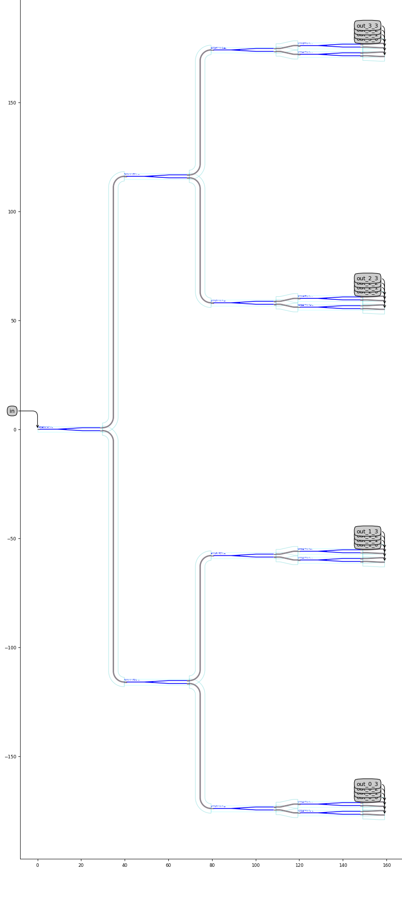
ShuksanSplitterTree
Custom splitter tree for the SiEPIC Shuksan PDK, where the vertical spacing of the output waveguides is not constant. The output waveguides are distributed over several waveguide groups in which the waveguides are closer together than the vertical distance between those groups. Circuit model is derived from the hierarchical model.
- Parameters:
- wg_radius: float and number > 0
Radius of the routed waveguide bends
- splitter: PCell
Splitter used
- spacing_y_groups: float and number > 0
Vertical spacing between the groups
- spacing_y_ports: float and number > 0
Vertical spacing between the output ports
- n_wg_groups: int
Number of grouped output waveguides (or sub splitter trees)
- n_wgs_per_wg_group: int
Number of waveguides per group
- strict: ( bool, bool_ or int )
If True, any error will raise an exception and stop the program flow. If False, any routing error will give a warning and draw a straight line on an error layer. See
i3.ConnectLogicalfor more information.- exposed_ports: ( dict ), *None allowed*
Ports to be exposed, mapping {‘instance_name:port_name’: external_port_name’} map for i3.expose_ports().Set to None (default) to expose all unconnected ports
- specs: list
Placement and routing specifications
- insts: OrderedDict and key: str, value: PCell, _View
Instances of child cells which this circuit is composed of: {‘instance_name’: cell, …} where cell is an i3.PCell object.
- name: String that contains only ISO/IEC 8859-1 (extended ASCII py3) or pure ASCII (py2) characters
The unique name of the pcell
- Other Parameters:
- spacing_x: float and number > 0, locked
Horizontal spacing between the levels
- n_levels_ports: int, locked
Number of port levels within a group
- n_levels_groups: int, locked
Number of group levels
from siepic_shuksan import technology
from siepic_shuksan.all import ShuksanSplitterTree
lo = ShuksanSplitterTree().Layout()
lo.visualize(annotate=True, box=None, canvas_size=(1000.0, None))
Ports
Name |
Type |
Position |
Angle |
Waveguide Template |
Inclination |
|---|---|---|---|---|---|
in |
Optical |
(0.0,0.0) |
180.0 |
WaveguideWireTemplate |
0.0 |
out_0_0 |
Optical |
(159.164,-177.0) |
0.0 |
WaveguideWireTemplate |
0.0 |
out_0_1 |
Optical |
(159.164,-175.0) |
0.0 |
WaveguideWireTemplate |
0.0 |
out_0_2 |
Optical |
(159.164,-173.0) |
0.0 |
WaveguideWireTemplate |
0.0 |
out_0_3 |
Optical |
(159.164,-171.0) |
0.0 |
WaveguideWireTemplate |
0.0 |
out_1_0 |
Optical |
(159.164,-61.0) |
0.0 |
WaveguideWireTemplate |
0.0 |
out_1_1 |
Optical |
(159.164,-59.0) |
0.0 |
WaveguideWireTemplate |
0.0 |
out_1_2 |
Optical |
(159.164,-57.0) |
0.0 |
WaveguideWireTemplate |
0.0 |
out_1_3 |
Optical |
(159.164,-55.0) |
0.0 |
WaveguideWireTemplate |
0.0 |
out_2_0 |
Optical |
(159.164,55.0) |
0.0 |
WaveguideWireTemplate |
0.0 |
out_2_1 |
Optical |
(159.164,57.0) |
0.0 |
WaveguideWireTemplate |
0.0 |
out_2_2 |
Optical |
(159.164,59.0) |
0.0 |
WaveguideWireTemplate |
0.0 |
out_2_3 |
Optical |
(159.164,61.0) |
0.0 |
WaveguideWireTemplate |
0.0 |
out_3_0 |
Optical |
(159.164,171.0) |
0.0 |
WaveguideWireTemplate |
0.0 |
out_3_1 |
Optical |
(159.164,173.0) |
0.0 |
WaveguideWireTemplate |
0.0 |
out_3_2 |
Optical |
(159.164,175.0) |
0.0 |
WaveguideWireTemplate |
0.0 |
out_3_3 |
Optical |
(159.164,177.0) |
0.0 |
WaveguideWireTemplate |
0.0 |
Layout
Parameters
- view_name: String that contains only alphanumeric characters from the ASCII set or contains _$. ASCII set is extended on PY3.
The name of the view
CircuitModel
Parameters
layout_view: ( _LayoutView ), None allowed netlist_view: ( NetlistView ), None allowed view_name: String that contains only alphanumeric characters from the ASCII set or contains _$. ASCII set is extended on PY3.
The name of the view
Other Parameters
- solver: str and String that contains only ISO/IEC 8859-1 (extended ASCII py3) or pure ASCII (py2) characters, locked
circuit solver to use
Tapers
taper_350nm_2000nm
Standard taper between the standard 350 nm and 2000 nm waveguide
from siepic_shuksan import technology
from siepic_shuksan.all import taper_350nm_2000nm
lo = taper_350nm_2000nm().Layout()
lo.visualize(annotate=True, box=None, canvas_size=(1000.0, None))

Ports
Name |
Type |
Position |
Angle |
Waveguide Template |
Inclination |
|---|---|---|---|---|---|
opt2 |
Optical |
(50.01,0.0) |
0.0 |
WaveguideWireTemplate |
0.0 |
opt |
Optical |
(0.01,0.0) |
180.0 |
WaveguideWireTemplate |
0.0 |
Terminators
terminator_1310
Terminator waveguide at 1310 nm
from siepic_shuksan import technology
from siepic_shuksan.all import terminator_1310
lo = terminator_1310().Layout()
lo.visualize(annotate=True, box=None, canvas_size=(1000.0, None))
Ports
Name |
Type |
Position |
Angle |
Waveguide Template |
Inclination |
|---|---|---|---|---|---|
opt1 |
Optical |
(0.0,0.0) |
0.0 |
WaveguideWireTemplate |
0.0 |
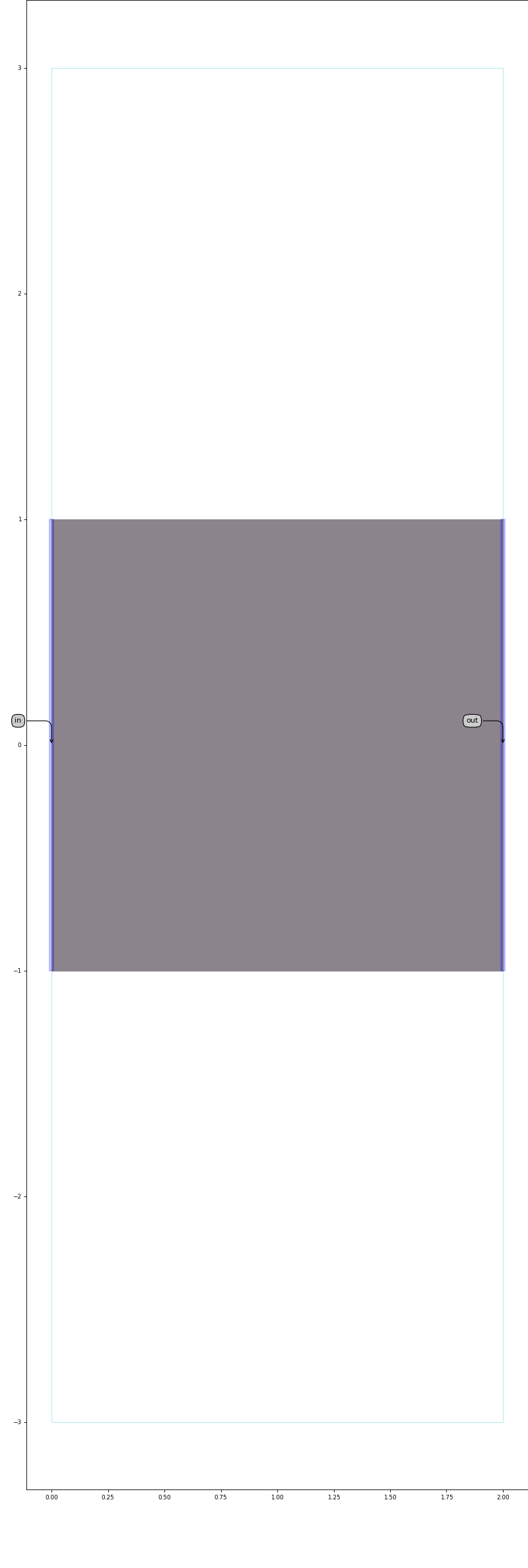
Waveguides
WaveguideWire
Waveguide wire where the core width can be user defined.
- Parameters:
- core_width: float and number > 0
Width of the core [um]
- trace_template: PCell and _WaveguideTemplate
- name: String that contains only ISO/IEC 8859-1 (extended ASCII py3) or pure ASCII (py2) characters
The unique name of the pcell
from siepic_shuksan import technology
from siepic_shuksan.all import WaveguideWire
lo = WaveguideWire().Layout()
lo.visualize(annotate=True, box=None, canvas_size=(1000.0, None))

Ports
Name |
Type |
Position |
Angle |
Waveguide Template |
Inclination |
|---|---|---|---|---|---|
in |
Optical |
(0.0,0.0) |
180.0 |
WaveguideWireTemplate |
0.0 |
out |
Optical |
(2.0,0.0) |
0.0 |
WaveguideWireTemplate |
0.0 |
Layout
Parameters
- core_width: float and number > 0
Width of the core [um]
- shape: Shape
Shape from which the Trace is calculated
trace_template: ( _LayoutView ), None allowed bend_radius: float and number > 0
Bend radius for the auto-generated bends.
CircuitModel
Parameters
- length: float and Real, number and number >= 0
The physical length of the waveguide during simulation
layout_view: ( _LayoutView ), None allowed netlist_view: ( NetlistView ), None allowed view_name: String that contains only alphanumeric characters from the ASCII set or contains _$. ASCII set is extended on PY3.
The name of the view
Other Parameters
- solver: str and String that contains only ISO/IEC 8859-1 (extended ASCII py3) or pure ASCII (py2) characters, locked
circuit solver to use
wg_strip_o_350
Standard single mode waveguide with a core width of 350 nm
- Parameters:
- name: String that contains only ISO/IEC 8859-1 (extended ASCII py3) or pure ASCII (py2) characters
The unique name of the pcell
from siepic_shuksan import technology
from siepic_shuksan.all import wg_strip_o_350
lo = wg_strip_o_350().Layout()
lo.visualize(annotate=True, box=None, canvas_size=(1000.0, None))
Ports
Name |
Type |
Position |
Angle |
Waveguide Template |
Inclination |
|---|---|---|---|---|---|
in |
Optical |
(0.0,0.0) |
180.0 |
WaveguideWireTemplate |
0.0 |
out |
Optical |
(2.0,0.0) |
0.0 |
WaveguideWireTemplate |
0.0 |
Layout
Parameters
- shape: Shape
Shape from which the Trace is calculated
- name: String that contains only ISO/IEC 8859-1 (extended ASCII py3) or pure ASCII (py2) characters
The unique name of the pcell
- bend_radius: float and number > 0
Bend radius for the auto-generated bends.
CircuitModel
Parameters
- length: float and number > 0
Length of the trace [micron]
- loss_db_per_cm: float and number > 0
Waveguide propagation loss [dB/cm]
- wavelength_bounds: ndarray
Wavelength range in which the model is valid
- ng_fit_coeff: ndarray
Fit coefficients of the group indices
- neff_fit_coeff: ndarray
Fit coefficients of the effective indices
layout_view: ( _LayoutView ), None allowed netlist_view: ( NetlistView ), None allowed view_name: String that contains only alphanumeric characters from the ASCII set or contains _$. ASCII set is extended on PY3.
The name of the view
Other Parameters
- solver: str and String that contains only ISO/IEC 8859-1 (extended ASCII py3) or pure ASCII (py2) characters, locked
circuit solver to use
wg_strip_o_mm_2000
Standard multimode waveguide with a core width of 2000 nm
- Parameters:
- name: String that contains only ISO/IEC 8859-1 (extended ASCII py3) or pure ASCII (py2) characters
The unique name of the pcell
from siepic_shuksan import technology
from siepic_shuksan.all import wg_strip_o_mm_2000
lo = wg_strip_o_mm_2000().Layout()
lo.visualize(annotate=True, box=None, canvas_size=(1000.0, None))
Ports
Name |
Type |
Position |
Angle |
Waveguide Template |
Inclination |
|---|---|---|---|---|---|
in |
Optical |
(0.0,0.0) |
180.0 |
WaveguideWireTemplate |
0.0 |
out |
Optical |
(2.0,0.0) |
0.0 |
WaveguideWireTemplate |
0.0 |
Layout
Parameters
- shape: Shape
Shape from which the Trace is calculated
- name: String that contains only ISO/IEC 8859-1 (extended ASCII py3) or pure ASCII (py2) characters
The unique name of the pcell
- bend_radius: float and number > 0
Bend radius for the auto-generated bends.
CircuitModel
Parameters
- length: float and number > 0
Length of the trace [micron]
- loss_db_per_cm: float and number > 0
Waveguide propagation loss [dB/cm]
- wavelength_bounds: ndarray
Wavelength range in which the model is valid
- ng_fit_coeff: ndarray
Fit coefficients of the group indices
- neff_fit_coeff: ndarray
Fit coefficients of the effective indices
layout_view: ( _LayoutView ), None allowed netlist_view: ( NetlistView ), None allowed view_name: String that contains only alphanumeric characters from the ASCII set or contains _$. ASCII set is extended on PY3.
The name of the view
Other Parameters
- solver: str and String that contains only ISO/IEC 8859-1 (extended ASCII py3) or pure ASCII (py2) characters, locked
circuit solver to use
Waveguide Bragg Gratings
WaveguideBraggGrating
Parametric Waveguide Bragg Grating (WBG). In this WBG, you can include chirp, apodization, an offset between the gratings on both sides of the waveguide, and you can choose between a rectangular or sinusoidal grating. The gratings have a standard duty cycle of 50%, but this can be adapted (only for the rectangular grating).
- Parameters:
- apodized: ( bool, bool_ or int )
Cosine apodization
- corrugation_width: float
Corrugation width [um]
- grating_chirp: float
Linear chirp parameter of the grating, meaning the difference in grating period at start and end [um]
- grating_duty_cycle: float and number > 0 and ]0.0,1.0[
Factor for the wide section (width of the wide section divided by grating period)
- grating_offset: float and Real, number and number >= 0
Horizontal offset between top and bottom grating
- grating_period: float and number > 0
Grating period at the center unit cell(s) [um]
- grating_shape: str and String that contains only ISO/IEC 8859-1 (extended ASCII py3) or pure ASCII (py2) characters and List with value restriction, allowed values: (‘RECT’, ‘SINE’)
Rectangular (‘RECT’) or sine (‘SINE’) grating
- n_periods: int and number >= 0
Number of periods
- width: float and number > 0
Average width of the grating [um]
- name: String that contains only ISO/IEC 8859-1 (extended ASCII py3) or pure ASCII (py2) characters
The unique name of the pcell
from siepic_shuksan import technology
from siepic_shuksan.all import WaveguideBraggGrating
lo = WaveguideBraggGrating().Layout()
lo.visualize(annotate=True, box=None, canvas_size=(1000.0, None))
Ports
Name |
Type |
Position |
Angle |
Waveguide Template |
Inclination |
|---|---|---|---|---|---|
pin1 |
Optical |
(0.0,0.0) |
180.0 |
WaveguideWireTemplate |
0.0 |
pin2 |
Optical |
(3.0,0.0) |
0.0 |
WaveguideWireTemplate |
0.0 |
Changelog
0.2.3.luceda4
Removed the use of PlaceRelative and replace it with Place(…, relative_to=…) for compatibility with Luceda 2024.09 and higher
Updated auto transition naming
0.2.3.luceda3
Use np.int32 instead of np.int for compatibility with numpy 1.26
Use np.float64 instead of np.float for compatibility with numpy 1.26
0.2.3.luceda2
Added an .iclib file (library file recognized by IPKISS Canvas) with symbol drawings
0.2.3.luceda1
Updated for IPKISS 3.9. The PDK runs on Python3 as well as Python2 IPKISS 3.9 is required to run the PDK
0.2.3
Fix snapping issues in the spirals and rings
Fix circuit model of the generic waveguide templates (and associated semi-autoroute waveguides)
Add Waveguide Bragg Grating parametric cell (only layout) and Terminator building block (only layout)
Add Heated Ring Filter parametric cells (only layout)
0.1.3
Initial implementation of the IPKISS PDK for SiEPIC Shuksan: layers, cell library, tape-out settings, basic documentation