Edge coupler
SiFab contains a nitride edge coupler:
SiNInvertedTaper: an inverted taper with customisable layout.
SiNInvertedTaper
This is an inverted taper with fully customisable layout.
The layout of this device and its default dimensions are taken from the following from the following paper [1].
The trace template of the port connecting it to the wider circuit can be set at PCell level with the parameter trace_template.
The remaining dimensions of the edge coupler can be set using the following parameters of the layout view: shallow_taper_start_width, shallow_taper_end_width, shallow_taper_length, shallow_straight_section_length, deep_straight_section_length, deep_taper_start_width, deep_taper_length.
This class has a circuit model to which the insertion_loss can be provided as a parameter in order to perform a circuit simulation.
Its default value is also given by [1].
Reference
Click on the name of the component below to see the complete PCell reference.
Inverted taper on an SiN platform. |
Example
import si_fab.all as pdk
from ipkiss3 import all as i3
import numpy as np
import pylab as plt
trace_template = pdk.NWG1000()
fc = pdk.SiNInvertedTaper()
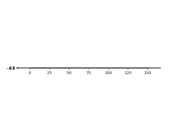
fc_lv = fc.Layout(
shallow_taper_start_width=0.75,
shallow_taper_end_width=1.0,
shallow_taper_length=45,
shallow_straight_section_length=1,
deep_straight_section_length=5,
deep_taper_start_width=0.6,
)
fc_lv.visualize()
fc_cm = fc.CircuitModel()
wavelengths = np.linspace(1.55, 1.56, 1000)
S = fc_cm.get_smatrix(wavelengths=wavelengths)
plt.figure()
plt.plot(wavelengths, i3.signal_power_dB(S["out", "in"]))
plt.xlabel("Wavelengths ($\\mu$m)")
plt.ylabel("Transmission (dB)")
plt.title("power transmission")
plt.show()
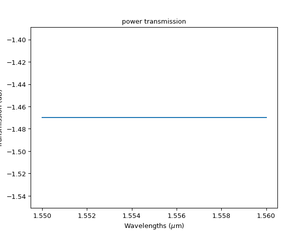
InvertedTaperModel
Inverted tapers are quite broadband. For the purpose of circuit model simulation, we assume that the insertion loss is constant with wavelength.