3. Build the behavioral model of an EAM
In the previous section, we demonstrated how to set up a separate python environment for nextnano. In this section, we will illustrate how to build the behavioral model of the absorption spectra for the QCSE-based EAM. We will proceed through the following steps:
Creating a multiple quantum well (MQW) stack and simulating its properties using the physical simulator provided by the software partner nextnano.
Calculating the absorption spectra of the QCSE-based EAM for different wavelengths and bias voltages.
Fitting the absorption spectra with a rational function model.
As a first step, we need to create and simulate the active layer of the modulator, which is the most essential part of the device. The MQW stack is sent to the nextnano software which specializes in solving the physics of quantum structures. This process is facilitated through an automated link available in the example code for this application case. The optical absorption of the MQW stack is calculated, and the simulation results are then used together with CAMFR, Luceda’s built-in EME solver, to determine the actual absorption of the optical mode when the MQW structure is integrated into a waveguide. We simulate the absorption for different voltage biases to incorporate the modulation behavior in the circuit model.
In the next step, we will fit the simulation data of the absorption using a rational function model. These rational functions and their associated fitting coefficients will be used in the circuit model for the QCSE-based EAM. The circuit model does not rely on interpolating the raw absorption data from the IPKISS/nextnano simulations, but instead utilizes a rational function with only a few coefficients. As a result the speed and memory usage of the circuit model is greatly optimized.
After obtaining the fitting data for the QCSE-based EAM circuit model, we can finally design a circuit based on this EAM device, which will be presented in the next section.
Note
The code in this application case utilizes an automated link between IPKISS and nextnano. It is to a large extent a generic link which can be used for other types of devices with some tweaking. It also serves as an example of how to link with a simulation tool that runs in a separate Python environment.
3.1. Creating a MQW material stack and run nextnano simulations
To start modeling the absorption spectrum of a QCSE-based EAM, we have to create the active layer of the component, which is the MQW material stack, and simulate the optical properties of the MQW stack.
We can define an MQW stack using the generate_EAM_material_stack function in the example script eam_stack.py.
This function is designed to define the active region of material stack for a QCSE-based EAM.
In the generate_EAM_material_stack function, we have to provide the parameters of the MQW, such as the height of the wells and barriers, material, doping, number of QWs, etc. In this tutorial, the parameters of the MQW structure follow the results of Lever et al. [1].
import si_fab.all as pdk  # noqa
import matplotlib.pyplot as plt
import numpy as np
import os
from ipkiss.visualisation.color import COLOR_BLUE as COLOR_DARK_BLUE
from ipkiss.visualisation.color import COLOR_RED as COLOR_LIGHT_RED
from ipkiss.visualisation.color import COLOR_GREEN as COLOR_SEA_GREEN
from pysics.basics.material.material_stack import MaterialStack
from ipkiss.visualisation.display_style import DisplayStyle
from scipy.interpolate import RegularGridInterpolator

from nextnano_link.simulation import (
    NextNanoSimulation1D,
    NextNanoOutput,
)
from nextnano_link.material import OpticalMaterial

from si_fab.technology.material_data import si_n_data, si_k_data, sio2_n_data
from eam_stack import generate_EAM_material_stack
from eam_handler import ElectroAbsorptionModulatorHandler

import pickle

curdir = os.path.dirname(__file__)

# Define a folder where to store our processed data
output_data = os.path.join(curdir, "output_data")

# Create a MQW stack
EAM_stack = generate_EAM_material_stack(
    number_of_wells=10,
    barrier_height=0.013,
    well_height=0.008,
    buffer_height=0.5,
    spacer_height=0.02,
    cap_height=0.1,
    Ge_buffer=0.7,
    Ge_well=1.0,
    Ge_barrier=0.6,
    Ge_cap=0.7,
    doping_cap=-7e18,
    doping_buffer=7e18,
)

MQW_height = EAM_stack.solid_height

# Visualize the MQW stack
# from nextnano_link.material import visualize_material_stack
# visualize_material_stack(EAM_stack)
After creating the MQW layer, we proceed to simulating its optical properties.
Users can define the specifications of the MQW within IPKISS and use an automated link to pass the simulation to nextnano.
For the purpose of this application example, we defined a class NextNanoSimulation1D that allows to define and run a simulation on a layer stack with nextnano from IPKISS. In this class, we have to specify the MQW stack, z-grid (simulation resolution), voltage bias, and the wavelength range. Subsequently, the simulation results of the MQW stack are retrieved, automatically returning the results to IPKISS.
In this way, we can find the optical properties as a function of wavelength, including the real and imaginary parts of the overall permittivity, which describe the MQW optically as if it were a uniform medium (see later).
Please find the full code of NextNanoSimulation1D in nextnano_link/simulation.py.
wavelength_range = [1.26, 1.36, 250]

# Setting up the nextnano simulation
simjob = NextNanoSimulation1D(
    material_stack=EAM_stack,
    project_folder="output_data",
    project_file_basename="EAM_output_nobias",
    input_file_template=os.path.join(curdir, "nextnano_link", "input_template1D_SiGe_EAM.txt"),
    outputs=[NextNanoOutput(name="built_in_at_0bias", output="built_in_potential")],
    z_grid=0.0001,
    run=["strain", "current_poisson", "quantum"],
    bias=0.0,
    # field=0,  # 1.5e7,  # in V/m
    spectrum=wavelength_range,
    variables_dict={
        "QuantumRegionMin": EAM_stack.quantum_region_min * 1000,
        "QuantumRegionMax": EAM_stack.quantum_region_max * 1000,
    },  # factor 1000 to convert to nm
)

# Inspect the nextnano simulation, or rather, inspect the InputFile
simjob.inspect()

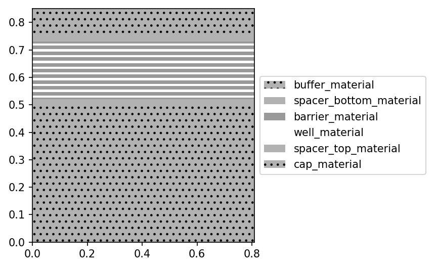
Visualization of the multiple quantum wells stack created by the generate_EAM_material_stack function.
3.2. Creating an absorption spectrum model of the QCSE-based EAM as a function of different voltage biases
In this part of the application example, we will demonstrate how to build an absorption spectrum model of the QCSE-based EAM that takes into account the optical properties at different bias voltages. There are 3 steps to build the absorption spectrum model:
- Construct the cross section of the QCSE-based EAM
Create the MQW stack:
We create the active MQW stack of the modulator and then simulate the absorption using the IPKISS/nextnano link.
Create the material stacks of the QCSE-based EAM waveguide:
We define all the materials that exist in the cross section of the QCSE-based EAM waveguide, including the Si waveguide and SiO2 cladding layers. The QCSE-based EAM now is a waveguide-like structure with the optical input-output ports and optical coupling structures.
    # Define materials: Si, SiO2, and MQW  (we regard a MQW stack as single material with uniform properties)
    si = OpticalMaterial(
        name="silicon",
        display_style=DisplayStyle(color=COLOR_LIGHT_RED),
        n=si_n_data,
        k=si_k_data,
    )
    ox = OpticalMaterial(
        name="oxide",
        display_style=DisplayStyle(color=COLOR_DARK_BLUE),
        n=sio2_n_data,
    )
    MQW_material = OpticalMaterial(
        name="MQW",
        n=nextnano_data_n,
        k=nextnano_data_k,
        display_style=DisplayStyle(color=COLOR_SEA_GREEN),
    )

    # Create material stacks
    # First stack is the passive region of the EAM, which is etched-SOI waveguide
    soi_etched = MaterialStack(
        name="soi_etched",
        materials_heights=[(ox, 2.0), (si, 0.22), (ox, 1.0)],
        display_style=DisplayStyle(color=COLOR_DARK_BLUE),
    )

    # Second stack is the active region of the EAM, which contains the multiple quantum wells structure
    core = MaterialStack(
        name="core",
        materials_heights=[(ox, 2.0), (si, 0.22), (MQW_material, MQW_height), (ox, 0.548)],
        display_style=DisplayStyle(color=COLOR_SEA_GREEN),
    )  # core and cladding stacks are defined
- Simulate the optical properties of the QCSE-based EAM waveguide by effective index method
We use CAMFR (an EME solver in IPKISS) to simulate the effective permittivity of all the stacks
- Calculate the absorption spectrum per unit length
Once we get the effective permittivity of the whole EAM structure, the QCSE-based EAM absorption per unit length can be easily determined from the imaginary part of the effective index.
In this application example, we defined a class ElectroAbsorptionModulatorHandler, which is responsible for steps 2 and 3. The purpose of the ElectroAbsorptionModulatorHandler is to calculate the absorption spectrum per unit length. Once we specify the material stacks and all its dimensions, the class will calculate the the effective index of the QCSE-based EAM with the effective index method. Then it will estimate the absorption spectrum of the EAM per unit length.
    # Modeling the EAM based on the material stacks
    EAM = ElectroAbsorptionModulatorHandler(
        core_stack=core,
        cladding_stack=soi_etched,
        core_width=0.5,
        cladding_width=2.0,
        length=60,
    )

    # EAM.visualize()
    # EAM.visualize_2d()

    # Store the information of bias, wavelength, and absorption under certain bias and certain wavelength
    alpha = EAM.calculate_absorption(
        wavelengths=wavelengths,
        mode="TE0",
        save_file=os.path.join(output_data, f"Alpha_dB_mu_{applied_bias}.csv"),
    )
    eam_pl_data.append(alpha)
    wavelength_data.append(wavelengths)
    bias_data.append([np.float64(bias)] * len(wavelengths))

    plt.xlabel("Wavelength(nm)")
    plt.ylabel("Absorption(dB)")
    plt.title(f"Absorption spectrum of a QCSE-based EAM under -{applied_bias}V bias")
    plt.plot(wavelengths, alpha)
    plt.grid(True)
    plt.show()
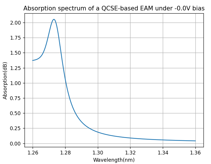
The image below shows the absorption spectrum of the QCSE-based EAM under the built-in potential bias of 0 V bias. There is clearly an absorption peak at around 1273nm, then the absorption becomes weaker as the wavelength increases.

Absorption spectrum of the QCSE-based EAM as a function of wavelength at 0 V reverse bias.
For more details on the ElectroAbsorptionModulatorHandler and on the calucation of the absorption spectrum, see luceda_academy/training/topical_training/nextnano_eam_simulation/nextnano_eam/eam_handler.py.
3.3. Setting the interpolation method for the absorption spectrum model of the QCSE-based EAM
When designing a circuit containing an EAM, one may want to simulate it at different wavelengths or voltage biases in comparison to the device initially simulated for obtaining the model data. For example, if the absorption spectra were determined at -1 V and 0 V bias voltage, you might want to simulate the modulator’s behavior at an intermediate -0.5 V. To address this, we will physically simulate the EAM under different biases, then we will interpolate over the results and use these interpolated results in the circuit model of the EAM.
We save the absorption spectrum data of the QCSE-based EAM in function of bias in a text file. We separately save the wavelengths and bias voltages for which the QCSE-based EAM is simulated and we store it as lists so that we reuse the data for circuit simulations. We use the RegularGridInterpolator from the package scipy to execute the interpolation. This creates Python object that takes the desired wavelengths and biases as inputs and returns the interpolated value from the data. We want to reuse the data in later scripts, which means that we can save it and load that object in the other scripts. For that, one can use the module pickle.
Then, we use the interpolator to calculate the interpolated values for each data point in the corresponding wavelength for a list of different biases. Note that we can’t run circuit simulations with a voltage or wavelengths outside the range at which the QCSE-based EAM was physically simulated. Thus the wavelength and bias range for absorption coefficients is something to consider before physical device simulations.
# Save the wavelength, bias, and absorption data to .txt file, which will be used for fitting
bias_data = np.hstack(np.float64(bias_data))
eam_pl_data = np.hstack(np.float64(eam_pl_data))

np.savetxt(os.path.join(output_data, "Wavelength_data_nnsim.txt"), wavelengths, delimiter=",")
np.savetxt(os.path.join(output_data, "Bias_data_nnsim.txt"), bias_data, delimiter=",")
np.savetxt(os.path.join(output_data, "Eam_pl_data_nnsim.txt"), eam_pl_data, delimiter=",")

# To load these files you can do the following:
wavelengths = np.loadtxt(os.path.join(output_data, "Wavelength_data_nnsim.txt"))
bias_data = np.loadtxt(os.path.join(output_data, "Bias_data_nnsim.txt"))
eam_pl_data = np.loadtxt(os.path.join(output_data, "Eam_pl_data_nnsim.txt"))


data = np.array(
    [
        # load each file
        np.loadtxt(os.path.join(output_data, f"Alpha_dB_mu_{bias}.csv"), delimiter=",")
        for bias in bias_list
    ]
)

interpolator = RegularGridInterpolator((bias_list, wavelengths), data, method="cubic")

with open(os.path.join(output_data, "interpolator.pkl"), "wb") as interpolator_pkl:
    pickle.dump(interpolator, interpolator_pkl)

absorption = []
simulated_biases = bias_list
new_bias = np.sort(np.append(np.array([0.5, 1.5, 2.5]), simulated_biases))
for new_b in new_bias:
    points_to_interpolate = np.column_stack([new_b * np.ones(len(wavelengths)), wavelengths])
    interpolated_abs_values = interpolator(points_to_interpolate)
    absorption.append(interpolated_abs_values)

for i, bias in enumerate(new_bias):
    plt.plot(
        wavelengths,
        absorption[i],
        "-" if bias in simulated_biases else "--",
        label=f"Bias -{bias} V (Interpolation)" if bias in simulated_biases else f"Actual Bias -{bias} V (Simulation)",
    )
plt.xlabel("Wavelength(nm)")
plt.ylabel("Absorption(dB)")
plt.title("Absorption spectrum of the QCSE-based EAM under different interpolated Bias Values")
plt.legend()
plt.grid(True)
plt.show()
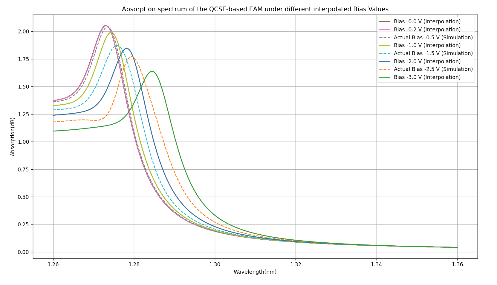
The image below shows the absorption spectra for various interpolated biases as a function of the wavelength. The solid curves in the plot are results from the nextnano simulations, while the dashed lines are interpolated results from these simulations.

The simulated and interpolated absorption spectra of the QCSE-based EAM. The solid curves are the absorption spectra simulated by nextnano. The dashed lines are the interpolated ones for various voltage biases.