1. Introduction
Field-programmable gate arrays (FPGAs) are well-known circuits in the integrated electronics world [1].
![FPGA schematic. Image from [2]_ (|CC_BY_4.0|).](../../../_images/FPGA-Graphics.jpg)
FPGA schematic, showing the CLBs placed in a switching matrix. Image from [2] (CC BY 4.0).
Their name comes from the fact that the functionality of these circuits can be reconfigured by the customer after they have been fabricated by the foundry. In particular, the FPGA consists of configurable logic blocks (CLBs) and a switching matrix that connects these logic blocks together. The key here is that both the CLBs and the switching matrix are programmable by means of applying voltages at specific switches in the CLBs and switching matrix. This way, the functionality of the CLBs and the way they are connected together can be changed by the user after the chip has been manufactured; the user simply has to apply the correct voltages at the correct switches in the FPGA (which is generally done through a hardware description language) in order to realise its desired performance. Since FPGAs are reconfigurable, the same chip can be used in a wide range of industries and for a wide range of functionalities, such as image processing in MRI systems and machine learning in AI networks.
In recent years, the FPGA concept is increasingly being applied to photonic integrated circuits (PICs) as well [3]. These photonic chips are called field-programmable photonic gate arrays (FPPGAs) or programmable photonic circuits (PPCs) - we will use the latter notation for consistency. Some PPCs have already entered the stage of commercialisation, as e.g. the company iPronics has demonstrated [4]. The principle of the PPC is similar to the FPGA: by changing the voltages at specific switches, the functionality of the chip can be changed after it has been fabricated. The “CLB” or unit cell of the PPC is a 2x2 mach-zehnder interferometer (MZI) switch. Light at one of the inputs of the MZI can be redirected to both MZI outputs to a desired degree, by merely applying a voltage to the phase shifter in one of the MZI arms (see the MZI lattice filter tutorial for more information about MZI design).
In the context of programmable photonics, the switch has generally three states, or configurations:
bar: light from the bottom (top) MZI input port ends up at the bottom (top) MZI output port.
cross: light from the bottom (top) MZI input port ends up at the top (bottom) MZI output port.
coupler: light from one of the MZI input ports ends up at both the top and bottom MZI output ports (typically split evenly over both outputs, i.e. 50/50).
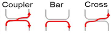
3 states of the MZI switch.
A PPC contains a lot of these MZI switches connected together in a triangular, square or hexagonal mesh (although forward-only topologies also exist) - for more information, see [3]. By changing the voltages on each of the switches, light can be dynamically rerouted on the PPC, and hence the functionality of the PPC can be reconfigured. PPCs have been shown to achieve tunable delay lines, reconfigurable microwave optical filters, tunable routing devices, beamforming networks, quantum optical neural networks, and many more [3]. Although the footprint of the MZIs and their connections is generally large, with a large PPC chip footprint as a result, using a low-footprint material platform such as silicon on insulator (SOI) or using novel MZI topologies can help downscaling the PPC size [5].
In this tutorial, we will show how to use Luceda IPKISS to design a rectangular PPC made in a SiN platform. In particular, we will show how the PPC MZI switches are connected and its optical and electrical I/O ports are routed to the edges of the chip. Then we will show how the same PPC design can be reconfigured to create a tunable delay line, a tunable routing network and a tunable microring filter.