2. The QKD Receiver
In this tutorial, we show how to create a receiver for quantum key distribution (QKD) in Luceda IPKISS. We implement the receiver circuit design from [1] which reads the quantum key from a series of pulses. This circuit is implemented in a nitride platform, which is important in order to minimize losses. A number of protocols for QKD can be implemented in this circuit:
BB84
Coherent one way (COW)
Differential phase shift (DPS)
In this tutorial, we will consider only the DPS protocol.
![Receiver for quantum key distribution. Image from [1]_ (|CC_BY_4.0|).](../../../_images/receiver_with_input.png)
Receiver for quantum key distribution. Image from [1] (CC BY 4.0).
2.1. How the circuit works
The QKD receiver circuit is composed of several building blocks:
The first MZI acts as a tunable beamsplitter (TBS), used primarily for the COW protocol (not in the scope of this tutorial).
The second MZI is a loss-balancing MZI (L-BAL), used to balance the losses in the two arms of the following MZI.
The third MZI is an asymmetrical MZI with a time delay in one arm, which is the core of the receiver circuit.
Let’s have a look at these building blocks one by one.
2.1.1. The input pulse train
At the input of the circuit (the second port on the left), a train of pulses is inputted that comes from the output of a QKD transmitter. This train of pulses contains the information for the quantum key. In the DPS protocol, the pulses are of equal amplitude and are equally spaced. The phase difference between them can be either \(0\) or \(\pi\). The quantum key is encoded in the phase difference.
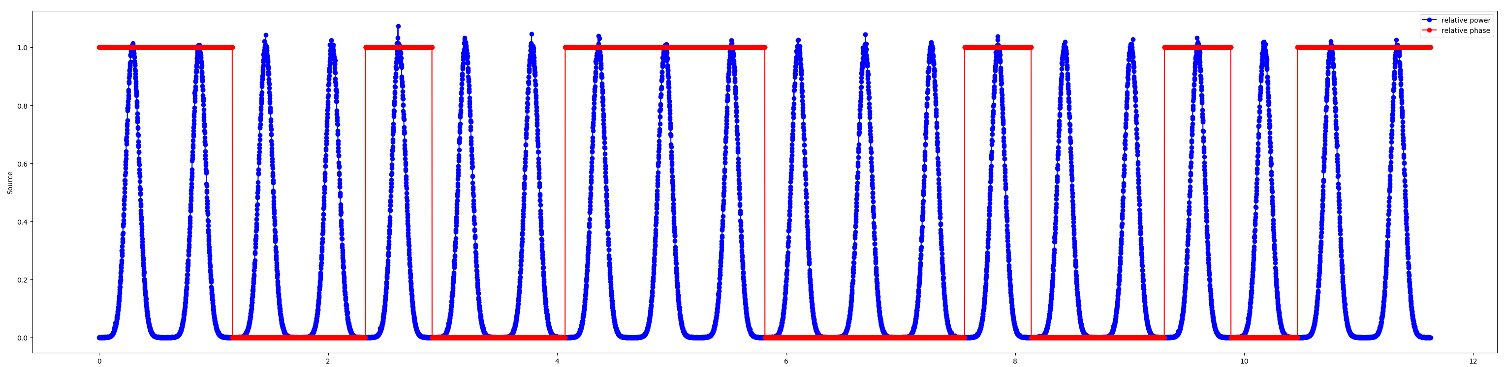
The input pulse train.
2.1.2. Asymmetric MZI with time delay
The most interesting physics in the circuit occurs in this part, which is an asymmetrical MZI with a time delay in one arm. At the input of the MZI, each of the pulses is split into two. For each pulse, one half propagates through the straight waveguide section whereas the other half passes through the delay line. The second half gets delayed long enough that it reaches the output directional coupler at the same time as the first half of the next pulse. The two halves of the subsequent pulses interfere at the directional coupler at the output of the MZI. Depending on whether they have the same or a different phase, the recombined pulses are detected at one or the other of the top two photodetectors in the figure below.
There are several tunable MZIs along the time delay that allow it to be reconfigurable. The total time delay can be of any integer multiple from \(1\) to \(7\) of the time delay defined by an individual spiral. The straight waveguide of the MZI also has a thermo-optic phase shifter, called TOPS, which is used to ensure that the phase difference between each half of one pulse remains the same at the output end of the MZI.
![Receiver for quantum key distribution. Image from [1]_ (|CC_BY_4.0|, has been modified).](../../../_images/receiver_td.png)
Asymmetric MZI with a time delay used in a receiver for quantum key distribution. Image from [1] (CC BY 4.0, has been modified).
2.1.3. MZI for loss balancing
For the circuit to correctly behave as described above, it is important to precede the asymmetrical MZI with a loss-balancing MZI (called L-BAL, see below). This is because, with 50/50 power splitting at the input of the asymmetrical MZI, the pulses at the input of the directional coupler at the output of the MZI would be of different amplitudes due to the different losses in the two paths. This would lead to incomplete interference between the two pulses and thus light being detected at both of the top two photodetectors (classically). Through the addition of a loss balancing MZI before the asymmetric MZI, it is possible to have variable power splitting at the input of the latter. We can thus find the point at which the total amplitudes at the input of the directional coupler are the same and thus the two pulses interfere completely.
![MZI used for loss balancing used in a receiver for quantum key distribution. Image from [1]_ (|CC_BY_4.0|, has been modified).](../../../_images/receiver_l-bal.png)
MZI used for loss balancing in a receiver for quantum key distribution. Image from [1] (CC BY 4.0, has been modified).
2.1.4. MZI used as tunable beam splitter
Finally, there is a tunable beam splitter (TBS) at the input of the circuit. In the COW protocol, some of the light is routed to the output photodetector at the bottom, but, for the protocol we are using, all light is routed to the loss balancing and tunable MZIs. The COW protocol is outside the scope of this tutorial.
![MZI used as a tunable beam splitter in a receiver for quantum key distribution. Image from [1]_ (|CC_BY_4.0|, has been modified).](../../../_images/receiver_tbs.png)
MZI used as a tunable beam splitter in a receiver for quantum key distribution. Image from [1] (CC BY 4.0, has been modified).
2.2. Implementation of the circuit in IPKISS
To create the circuit layout in IPKISS, we use components from the demo PDK SiFab, as well as from the the library pteam_library_si_fab. It is important that we use silicon nitride components, rather than silicon, so that we can take advantage of silicon nitride’s low losses.
To start, we import the following classes from the SiFab PDK:
A silicon nitride wire trace template (
NWG900)A silicon nitride directional coupler (
SiNDirectionalCouplerSPower)A heater (
HeatedWaveguide)
On top of this, we also import the following components that we implemented in the library pteam_library_si_fab:
An MZI (
MZI)A tunable delay line (
TunableDelayLine)
We then connect the components together using i3.Circuit:
class Receiver(i3.Circuit):
    """A receiver used for quantum key distribution. It takes a sequence of pulses as an input in which the key is
    encoded and interferes between them to output the values of the individual bits.
    """

    buffer_waveguide_length = i3.PositiveNumberProperty(
        doc="length of the buffer waveguide seperating the phase shifers from the couplers in the MZIs",
        default=10.0,
    )

    def _default_specs(self):
        trace_template = pdk.NWG900()
        phase_shifter = pdk.HeatedWaveguide(
            name=self.name + "_phase_shifter",
            trace_template=trace_template,
        )
        phase_shifter.Layout(shape=i3.Shape([(0, 0), (30, 0)]))
        coupler = pdk.SiNDirectionalCouplerSPower(
            name=self.name + "_coupler",
            power_fraction=0.5,
        )

        mzi = MZI(
            name=self.name + "_mzi",
            coupler=coupler,
            phase_shifter=phase_shifter,
            x_separation=self.buffer_waveguide_length,
            extra_y_separation=0,
        )

        delay = TunableDelayLine(
            name=self.name + "_tunable_delay",
            delay_time=2.1,
        )

        specs = [
            i3.Inst(["mzi1", "mzi2"], mzi),
            i3.Inst("delay", delay),
            i3.Inst("phase_shifter", phase_shifter),
            i3.Inst("coupler", coupler),
            i3.Place("mzi1:in1", (0, 0)),
            i3.Place("mzi2:in1", (self.buffer_waveguide_length, 0), relative_to="mzi1:out2"),
            i3.Place("phase_shifter:in", (3600, 0), relative_to="mzi2:out1"),
            i3.Place("delay:in1", (self.buffer_waveguide_length, 0), relative_to="mzi2:out2"),
            i3.Place("coupler:in2", (self.buffer_waveguide_length, 0), relative_to="delay:out1"),
            i3.ConnectManhattan(
                [
                    ("mzi2:in1", "mzi1:out2"),
                    ("phase_shifter:in", "mzi2:out1"),
                    ("delay:in1", "mzi2:out2"),
                    ("coupler:in1", "phase_shifter:out"),
                    ("coupler:in2", "delay:out1"),
                ]
            ),
        ]
        return specs

    def _default_exposed_ports(self):
        input_optical_ports = [
            "mzi1:in1",
            "mzi1:in2",
            "mzi2:in2",
            "delay:in2",
        ]

        output_optical_ports = [
            "mzi1:out1",
            "coupler:out1",
            "coupler:out2",
            "delay:out2",
        ]

        electrical_ports = [
            "mzi1:elec1",
            "mzi1:elec2",
            "mzi2:elec1",
            "mzi2:elec2",
            "delay:elec11",
            "delay:elec12",
            "delay:elec21",
            "delay:elec22",
            "delay:elec31",
            "delay:elec32",
            "phase_shifter:elec1",
            "phase_shifter:elec2",
            "delay:elec41",
            "delay:elec42",
        ]

        port_list_dict = {
            "in": input_optical_ports,
            "out": output_optical_ports,
            "elec": electrical_ports,
        }

        ep = {}

        for port_dict_key in port_list_dict.keys():
            port_list = port_list_dict[port_dict_key]
            for i, port in enumerate(port_list):
                ep[port] = f"{port_dict_key}{i + 1}"

        return ep
Let’s analyze the code above. First, we instantiate the different components that we use. These are the TBS and L-BAL MZIs, the delay line, the TOPS phase shifter and the output directional coupler. Then, we place them and connect them together using Manhattan connections. Finally, we define the external ports of the receiver. It has four input and four output optical ports and a large number of electrical ports.
Now, we route the receiver to edge couplers and bond pads using i3.place_and_route:
class RoutedReceiver(i3.PCell):
    """A receiver for quantum key distribution that is routed to edge couplers and bond pads."""

    dut = i3.ChildCellProperty(doc="Receiver that needs to be routed.")
    edge_coupler = i3.ChildCellProperty(doc="Edge coupler used.")
    bondpad = i3.ChildCellProperty(doc="Bondpad used.")
    edge_coupler_pitch = i3.PositiveNumberProperty(
        default=50,
        doc="The vertical separation between the edge couplers",
    )
    edge_coupler_distance_x = i3.PositiveNumberProperty(
        default=100,
        doc="The horizontal distance between the edge couplers and the receiver",
    )
    bondpad_pitch = i3.PositiveNumberProperty(
        default=580,
        doc="The horizontal separation between the bond pads",
    )
    bondpad_distance_y = i3.PositiveNumberProperty(
        default=500,
        doc="The vertical distance between the bond pads and the receiver",
    )
    wire_spacing = i3.PositiveNumberProperty(default=10.0, doc="spacing between the electrical wires")
    bend_radius = i3.PositiveNumberProperty(default=60.0, doc="bend radius of the bends")

    def _default_dut(self):
        return Receiver(name="receiver")

    def _default_edge_coupler(self):
        trace_template = pdk.NWG900()
        return pdk.SiNInvertedTaper(trace_template=trace_template, name="inverted_taper")

    def _default_bondpad(self):
        return pdk.BONDPAD_5050()

    class Layout(i3.LayoutView):
        def generate(self, layout):
            # place device under test and bondpads

            dut_size = self.dut.size_info()
            el_ports = self.dut.electrical_ports.x_sorted()
            n_el_ports = len(el_ports)
            bondpad = self.bondpad
            bondpad_size = bondpad.size_info()

            specs = [
                i3.Inst("dut", self.dut),
                i3.Place("dut:in1", (0, 0)),
            ]

            for cnt, port in enumerate(el_ports):
                bp_name = f"bp_{cnt + 1}"
                specs.append(i3.Inst(bp_name, bondpad))
                bp_x = dut_size.center[0] + (cnt + (1 - n_el_ports) / 2.0) * self.bondpad_pitch
                bp_y = dut_size.south - bondpad_size.north - self.bondpad_distance_y
                specs.append(i3.Place(bp_name, (bp_x, bp_y)))

            layout = i3.place_and_route(layout=layout, specs=specs)

            specs = []
            # Electrical routing
            dy = -bondpad_size.north - self.bondpad_distance_y / 2.0
            for cnt, port in enumerate(el_ports):
                bp_name = f"bp_{cnt + 1}"
                bp_position = layout[bp_name].position
                if port.position.x > bp_position.x:
                    dy -= self.wire_spacing
                else:
                    dy += self.wire_spacing

                c = i3.ConnectElectrical(
                    f"dut:{port.name}",
                    f"{bp_name}:m1",
                    start_angle=-90.0,
                    end_angle=90.0,
                    control_points=[i3.H(dy, relative_to="dut@S")],
                )
                specs.append(c)

            # Optical routing
            opt_ports_in = layout["dut"].optical_ports.west_ports.y_sorted()
            opt_ports_out = layout["dut"].optical_ports.east_ports.y_sorted()
            fc_y = layout["dut"].ports["in1"].position.y
            fc_x_in = dut_size.west - self.edge_coupler_distance_x
            fc_x_out = dut_size.east + self.edge_coupler_distance_x
            for cnt, (p_in, p_out) in enumerate(zip(opt_ports_in, opt_ports_out)):
                input_coupler_name = f"fb_in{cnt + 1}"
                output_coupler_name = f"fb_out{cnt + 1}"
                specs.append(i3.Inst(input_coupler_name, self.edge_coupler))
                specs.append(i3.Inst(output_coupler_name, self.edge_coupler))
                specs.append(
                    i3.Place(
                        f"{input_coupler_name}:out",
                        (fc_x_in, fc_y + cnt * self.edge_coupler_pitch),
                    )
                )
                specs.append(
                    i3.Place(
                        f"{output_coupler_name}:out",
                        (fc_x_out, fc_y + cnt * self.edge_coupler_pitch),
                        angle=180.0,
                    )
                )
                specs.append(
                    i3.ConnectBend(
                        [
                            (p_in, f"{input_coupler_name}:out"),
                            (p_out, f"{output_coupler_name}:out"),
                        ],
                        bend_radius=self.bend_radius,
                    )
                )

            layout = i3.place_and_route(layout=layout, specs=specs)

            return layout
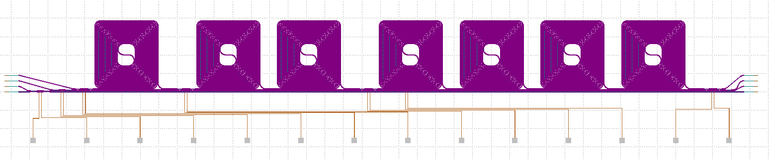
Layout of the QKD receiver.
2.3. Testbench and time-domain simulations
Now, we simulate our QKD receiver. We need to fist calculate the bias voltages applied to each of the individual phase-shifters in the circuit. Then, we simulate the receiver with these voltages applied in Caphe. We have defined two functions, bias_receiver and simulate_receiver, in which we do the above steps. In this example, we use these steps to simulate the circuit with a certain set of input parameters. The pulse train is inserted at the second input on the left hand side (see the layout in the previous section) whereas the key is read at the second and third output on the right hand side. We show the code for this example below:
import si_fab.all as pdk  # noqa: F401
import ipkiss3.all as i3
from qkd_receiver.receiver import Receiver
from qkd_receiver.test_and_tune_benches import bias_receiver, simulate_receiver
from scipy.constants import pi
import numpy as np
import matplotlib.pyplot as plt


########################################################################################################################
# Constants of for the biasing and simulation test benches
########################################################################################################################

opt_power = 5.0e-3
center_wavelength = 1.55
bitrate = 1.0 / 581.4e-12
plot_log = False
number_of_delays = 2
optical_noise = np.sqrt(0.003)


########################################################################################################################
# Bias the QKD receiver. The 4 different bias voltages are by default to None, which means that the bias voltages for
# optimum performance will be calculated automatically. If you don't want to optimize one particular biasing voltage,
# you just set that voltage to a certain value other than None.
########################################################################################################################

receiver_bias_voltages = bias_receiver(
    Receiver(),
    opt_amplitude=np.sqrt(opt_power),
    center_wavelength=center_wavelength,
    number_of_delays=number_of_delays,
    switch_voltage=None,
    lbal_voltage=None,
    tbs_voltage=None,
    tops_voltage=None,
)


########################################################################################################################
# Simulate the QKD receiver. Here, the bias voltages calculated in the previous step or given by the user are provided
# to the simulation test bench. This simulation test bench calculates the fields at the optical outputs of the
# receiver in case of the DPS protocol.
########################################################################################################################

results = simulate_receiver(
    Receiver(),
    opt_amplitude=np.sqrt(opt_power),
    opt_noise=optical_noise,
    bitrate=bitrate,
    center_wavelength=center_wavelength,
    bias_voltages=receiver_bias_voltages,
)


########################################################################################################################
# Plot the QKD receiver simulation results
########################################################################################################################

times = results.timesteps * 1e9
if plot_log:
    plt.subplot(211)
    plt.plot(times, 10.0 * np.log10(i3.signal_power(results["opt_src_in"]) / opt_power), "bo-", label="relative power")
    plt.plot(times, np.angle(results["opt_src_in"]) * (30.0 / pi) - 30.0, "ro-", label="relative phase")
    plt.ylabel("Source")
    plt.ylim([-30.0, 0.0])
    plt.legend()
    plt.subplot(212)
    plt.plot(times, 10.0 * np.log10(i3.signal_power(results["monitor_dl"]) / opt_power), "g-", label="Delay line tap")
    plt.plot(times, 10.0 * np.log10(i3.signal_power(results["monitor_plus"]) / opt_power), "bo-", label="|+>")
    plt.plot(times, 10.0 * np.log10(i3.signal_power(results["monitor_min"]) / opt_power), "ro-", label="|->")
    plt.ylabel("Relative power [dB]")
    plt.ylim([-30.0, 0.0])
    plt.legend()
else:
    plt.subplot(211)
    plt.plot(times, i3.signal_power(results["opt_src_in"]) / opt_power, "bo-", label="relative power")
    plt.plot(times, np.angle(results["opt_src_in"]) / pi, "ro-", label="relative phase")
    plt.ylabel("Source")
    plt.legend()
    plt.subplot(212)
    plt.plot(times, i3.signal_power(results["monitor_dl"]) / opt_power, "g-", label="Delay line tap")
    plt.plot(times, i3.signal_power(results["monitor_plus"]) / opt_power, "bo-", label="|+>")
    plt.plot(times, i3.signal_power(results["monitor_min"]) / opt_power, "ro-", label="|->")
    plt.ylabel("Relative power [a.u.]")
    plt.legend()
plt.xlabel("Time [ns]")
plt.legend()
plt.show()
Let’s analyze the code above. First, we provide some constants for which we simulate the circuit. These include a bitrate of 581.4 ps, which is the time difference between subsequent pulses. Since our tunable delay can be increased in steps of 300 ps for each spiral, we set number_of_delays = 2 to set the number of spirals the light passes through in the top arm of the asymmetric MZI to \(2\). This leads to a total delay of 600 ps which is similar to the bitrate. Using these inputs, we calculate each of the bias voltages needed using bias_receiver. Then, we call simulate_receiver to run the time-domain simulations using Caphe, the built-in circuit simulator in IPKISS. Finally, we plot the power measured at the outputs.
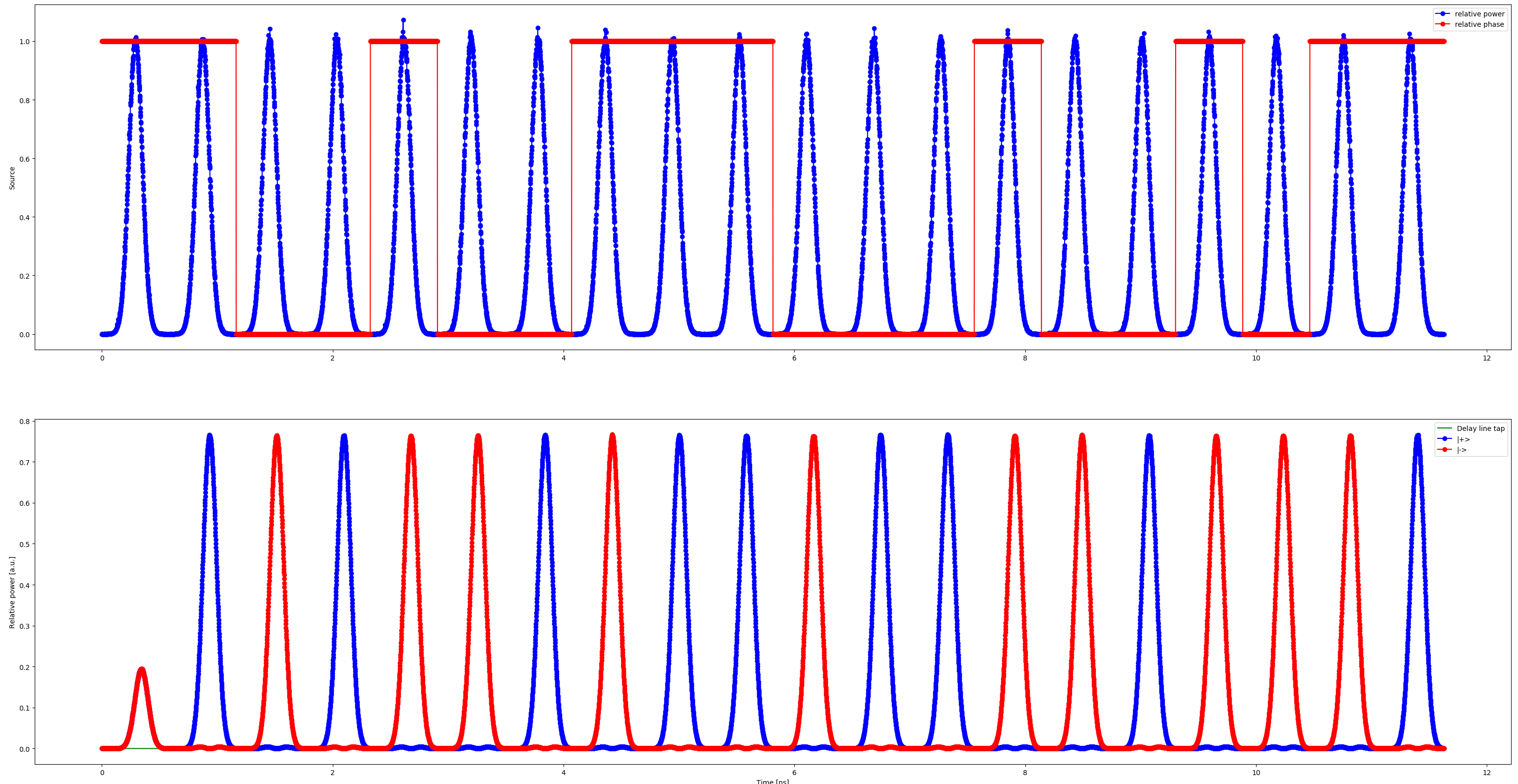
Results of time-domain simulations of the receiver.
2.4. Test your knowledge
Exercise 1: Effects of non-optimal loss balancing
As mentioned earlier, it is important that the pulses at the input of the directional coupler at the output of the asymmetrical MZI have the same amplitude. The simulation we have set up with IPKISS automatically calculates the optimal voltage, which corresponds to 1.04 V.
Open the file simulate_receiver.py.
On line 34, change the value of
lbal_voltageto a smaller value, such as 0.7 V.
receiver_bias_voltages = bias_receiver(
    Receiver(),
    opt_amplitude=np.sqrt(opt_power),
    center_wavelength=center_wavelength,
    number_of_delays=number_of_delays,
    switch_voltage=None,
    lbal_voltage=None,
    tbs_voltage=None,
    tops_voltage=None,
)
What happens to the optical output if the voltage applied to the loss balancing MZI is non-optimal? Is the simulation result what you expected?
Exercise 2: Effects of slightly detuning the bitrate
If the bitrate of the pulses is slightly detuned from the time delay, e.g. if the bitrate is reduced, the signal is going to be degraded.
Open the file simulate_receiver.py.
On line 16, change the value of
bitrateto a smaller value.
bitrate = 1.0 / 400.0e-12
What happens to the optical output? Is the simulation result what you expected?