Note
Go to the end to download the full example code
Finding overlapping elements in a layout
This example shows how to use layout operations to find and plot any overlaps between elements in a list of layers for a layout. This can be used to find accidental overlaps between waveguide or components that may cause a design to fail after fabrication.
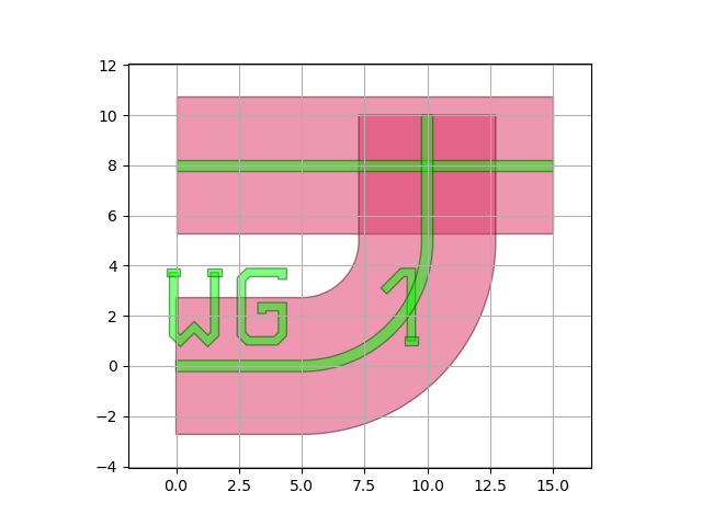
First we create a simple layout with some obvious errors:
import si_fab.all as pdk  # noqa
import ipkiss3.all as i3


class ExampleCircuit(i3.PCell):
    class Layout(i3.LayoutView):
        def generate(self, layout):
            layout += i3.SRef(reference=i3.RoundedWaveguide().Layout(shape=[(0, 0), (10, 0), (10, 10)]))
            layout += i3.SRef(reference=i3.RoundedWaveguide().Layout(shape=[(0, 8), (15, 8)]))

            layout += i3.PolygonText(
                layer=i3.TECH.PPLAYER.SI,
                coordinate=(5.0, 4.0),
                text="WG 1",
                height=3,
            )

            return layout


layout = ExampleCircuit().Layout()
layout.visualize()

The overlapping geometries in the layout can be checked using get_layer_overlaps function.
You pass in an IPKISS layout (which can be generated from a GDS file using
i3.GDSCell) as well as a list of layers. Any overlaps between geometries in each of
the layers in the list will be found. The function returns a python dictionary with the keys being the layers, and the
items for each key being the overlapping areas as IPKISS elements. We will use it to see if any over our waveguides
cross each other.
overlapping_elements = i3.get_layer_overlaps(layout, [i3.TECH.PPLAYER.SI])
We can print this dictionary to see how many overlaps there are. If there are no overlaps then we can have some confidence that none of our waveguides cross, or that any elements in this layer overlap.
print(overlapping_elements)
{<PPLayer SI-DRW>: [<Boundary on Layer PPLAYER SI-DRW>, <Boundary on Layer PPLAYER SI-DRW>, <Boundary on Layer PPLAYER SI-DRW>, <Boundary on Layer PPLAYER SI-DRW>, <Boundary on Layer PPLAYER SI-DRW>]}
There are actually five overlapping geometries, lets visualize them to see where they occur. To make them more visible we will use modified copy to create a copy of each element in the Silicon layer, and move it to the crossing error layer. Then we can visualize the list of error elements as well in the original layout. An i3.LayoutCell() is a lightweight way to create a new cell by passing in the elements of interest.
elems_in_error_layer = [
    b.modified_copy(layer=i3.TECH.PPLAYER.ERROR.CROSSING) for b in overlapping_elements[i3.TECH.PPLAYER.SI]
]

i3.LayoutCell().Layout(elements=layout.layout + elems_in_error_layer).visualize()

As expected we can see the places where the text overlaps the waveguide, and where the two waveguides cross.
However, we can also see that the generated text (using i3.PolygonText)
has some overlaps between the shapes of the letters. In a different layout we may also discover overlaps between
white-box components and waveguides, or other components, which could help us to create a design that works.
We could explore each of these boundaries further by accessing the boundary from the dictionary, then calling the shape and points to see the exact coordinates. For example “overlapping_elements[i3.TECH.PPLAYER.SI][0].shape.points” would return all the points of the first overlapping shape in the silicon layer from our dictionary.
A few things to note: This function will not detect a point or line where two or more geometries touch, without crossing each other. If you are using a PDK with black-box components, then you will be unable to detect overlaps between the hidden structures and other parts of your layout. You can pass in a list of layers to return all the overlaps in these layers. The output will be in the form of a python dictionary with a key for each layer you passed in. You cannot look for overlaps between different layers with this function directly. However, you could use modified_copy to move elements to a new layer then run the function again.