Release notes Luceda Photonics Design Platform 3.12.0
The Luceda 3.12 release brings significant improvements to the IPKISS Place & Route (P&R) engine. It becomes easier to place components and route optical and electrical wires relative to other objects in your design.
But that’s not all! Improvements enhance design efficiency and functionality across the whole platform:
Overlap detection, which can be used for instance to detect waveguide or metal line crossings.
Temperature-dependent circuit simulations and eye diagram support.
Visualization routines for circuit simulation results in frequency (S matrix) and time domain results (eye diagrams).
More detailed reporting during circuit simulation (progressbars and statistics on your simulation run).
Export of 3D object representation files (.stl, .mtl, .obj) of your layouts for verification and for interfacing with your favourite CAD tool.
Upgraded IPKISS Canvas symbol editor.
An example design of an IQ Modulator (layout + simulation) with simulations covering various modulation formats (OOK, BPSK, QPSK, PAM4, 16QAM).
Upgraded Python to Python 3.12.
For all features, bugfixes and improvements please consult the changelog.
Routing and layout improvements
As the complexity of photonic integrated circuits (PICs) keeps increasing, we are constantly adding and refining functionality to automate and simplify the Placement and Routing (P&R) process. Our P&R engine now includes the ability to describe relationships between routes and placed instances within your circuit. This enables easier avoidance of other devices or specific areas of your circuit, especially during waveguide and electrical wire routing. The result is a more expressive way to define your placement and routing problem, requiring less code and fewer manual calculations.
Here is an example where we use the relative routing (relative_to) in combination with the new anchors (N/E/S/W):
control_points=[
    i3.V(-20, relative_to="obstacle@W"),
    i3.H(20, relative_to="obstacle@N"),
    i3.V(20, relative_to="obstacle@E"),
],
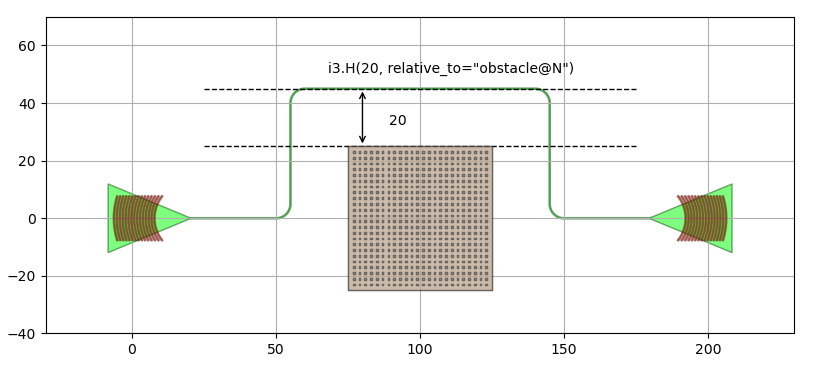
Control point using the new relative_to argument.
Here is another example using N/E/S/W anchors during placement. The specs that were used are these:
specs = [
    # Read: Place the south of mzi2 at 'distance' relative to the north of mzi1.
    i3.Place.Y("mzi2@S", distance, relative_to="mzi1@N"),
    i3.Place.Y("mzi3@S", distance, relative_to="mzi2@N"),
    i3.Place.Y("mzi4@S", distance, relative_to="mzi3@N"),
    # Read: Align all west sides of the instances vertically
    i3.AlignV(["mzi1@W", "mzi2@W", "mzi3@W", "mzi4@W"]),
]
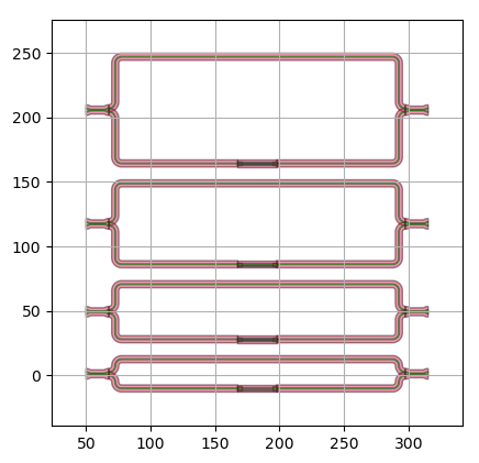
Placement of devices using N/E/S/W anchors.
Additionally, we have introduced a new electrical bundle connector to further automate the electrical routing process, making it easier to parametrize the routing in your complex circuits.

Routing of an electrical bundle with a single connector.
Samples & documentation:
Guide: Place & route specs.
Updated documentation:
i3.Place,i3.ConnectManhattan, and many more.Updated tutorials: Getting started in layout.
Electrical bundles:
i3.ConnectElectricalBundle.
Tape-out preparation
Preparing your layouts for tape-out is a critical step of the design flow, sometimes more time-consuming than the initial design process. To help you avoid common errors flagged by foundries’ design rule check (DRC), we have added a new functionality for detecting overlapping layers in your design. This proves particularly useful for detecting intersecting waveguides or cladding layers.
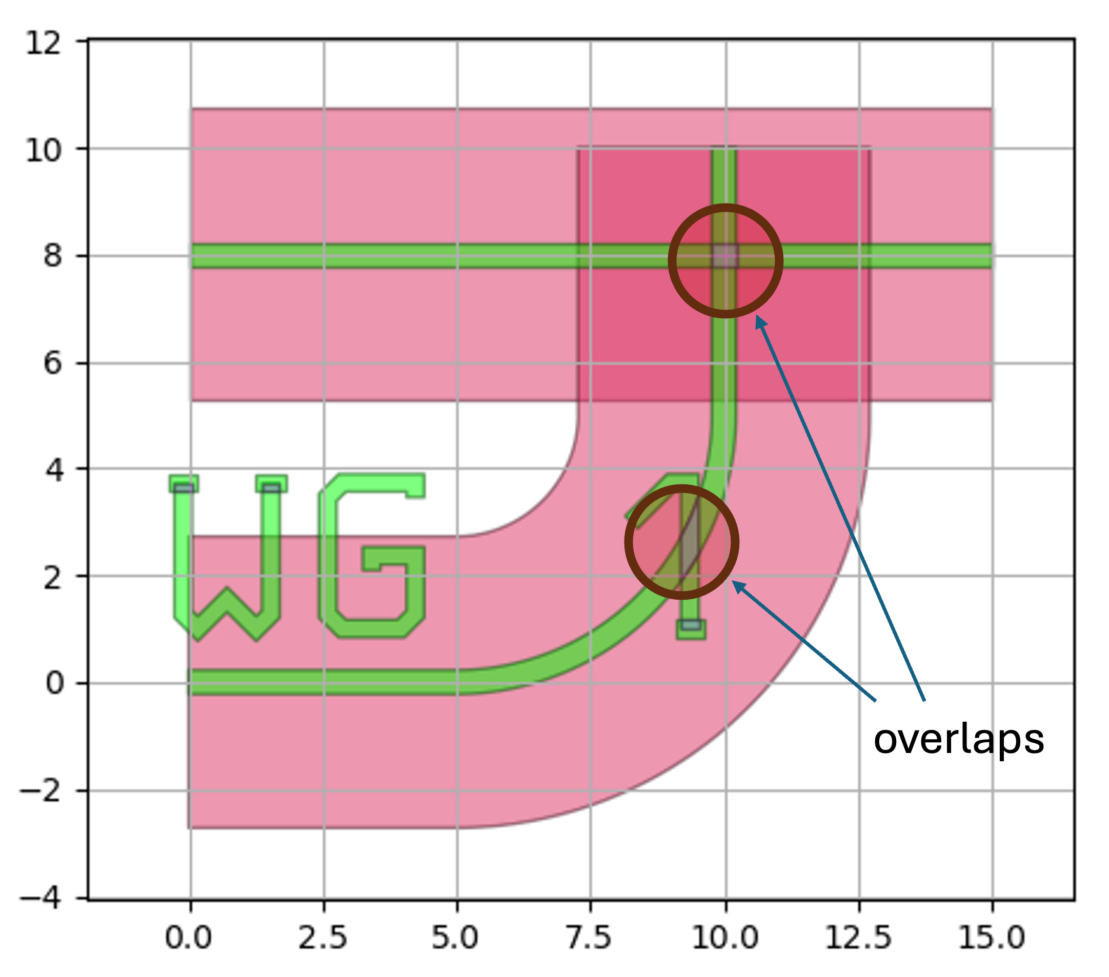
Detecting intersecting waveguides using the new overlap method.
Samples & documentation:
Check out our complete set of tape-out preparation features: layout operations.
Circuit simulation
Our circuit simulator, Caphe, now supports temperature-dependent circuit simulations, thanks to the addition of a new built-in global temperature environment variable.
We have introduced 2 types of S-matrix visualization (1D line graphs or 2D checkerboard plot) for frequency domain simulation (check out this sample), and eye diagrams for (large-signal transient) time-domain simulation.
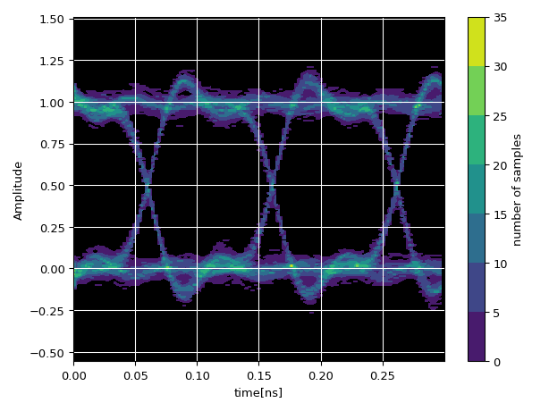
Eye diagram visualization from a time-domain circuit simulation.
When running simulations, Caphe can now provide additional statistics. For frequency domain, you can use a progress bar (this works both on the terminal and in jupyter notebooks). For frequency and time domain, you can also add more statistics about the matrix calculation and model execution time. While small-medium circuits execute very fast, this feature is valuable for advanced models and larger circuits.

Showing a progress bar and statistics on time execution during circuit simulation.
Progress bars are created using the tqmd package, which is now part of the Luceda IPKISS distribution. If you want to build your own progress bars, just wrap your for loop with a tqdm statement:
from tqdm import tqdm
from time import sleep

for i in tqdm(range(0, 100), total=500, desc="Simulation progress"):
    sleep(.1)
Samples & documentation:
New sample: Analyzing Kerr nonlinearity in optical ring resonators.
New sample: temperature-dependent simulation of a MZI.
New sample design: IQ Modulator (layout + simulation of various modulation formats).
Updated sample: Loading a touchstone file and plotting S-parameters.
Simulation visualization:
i3.EyeDiagram,i3.circuit_sim.SMatrix1DSweep.Simulation progressbar / statistics:
get_smatrixandget_time_response.
3D geometry export
With Luceda IPKISS users can export 3D geometries of IPKISS layout to supported simulation tools like Ansys Lumerical or CST Studio Suite for device-level simulations. We have now added support for STL and OBJ export formats - widely recognized as industry standards for defining 3D structures. This also exports the material data (MTL) which can be used by other CAD tools (for instance, to perform thermal / mechanical simulations).
With this new 3D geometry + material export functionality, you can import the 3D geometry of your IPKISS layouts into your preferred simulator, and even into PowerPoint! You can also use it to inspect your circuit with an extra dimensionality.
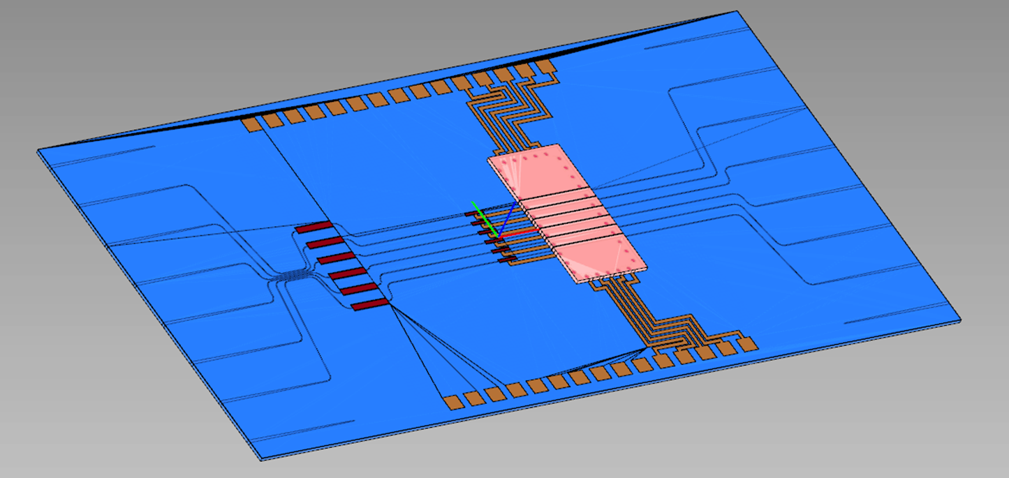
3D export of a photonic IC generated with the new write_obj and write_stl methods.
Samples & documentation:
Sample: Exporting a 3D Model file.
API reference:
i3.device_sim.SimulationGeometry.
IPKISS Canvas
This is the third release since we released IPKISS Canvas. We fixed several bugs related to some edge cases in rotations in Canvas, and the exporter from IPKISS to Canvas.
The symbol editor is now more compact and intuitive, making it easier to add and refine instance terms.
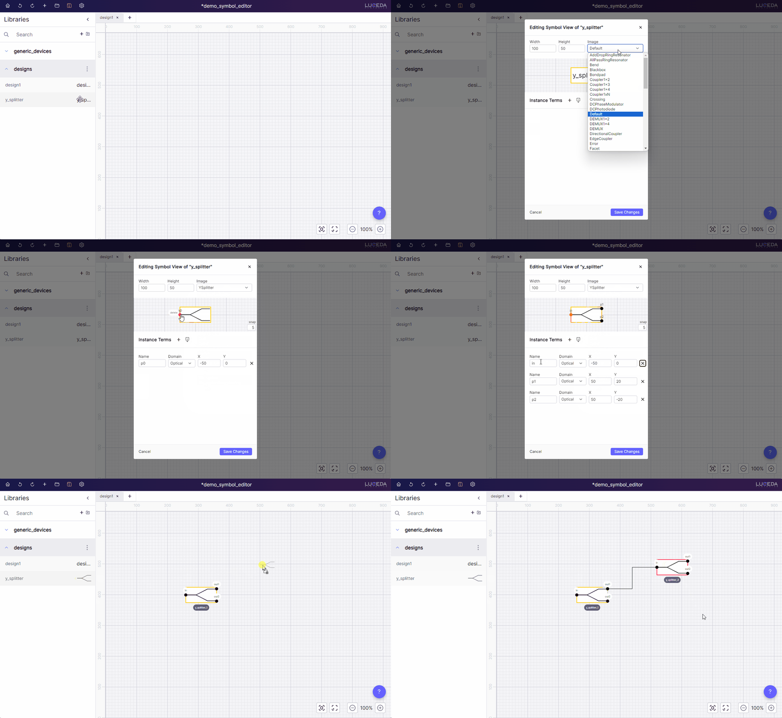
The symbol editor in IPKISS Canvas is now more compact and intuitive to use.
You can also copy terms from the schematic, saving time and avoiding duplicate work:
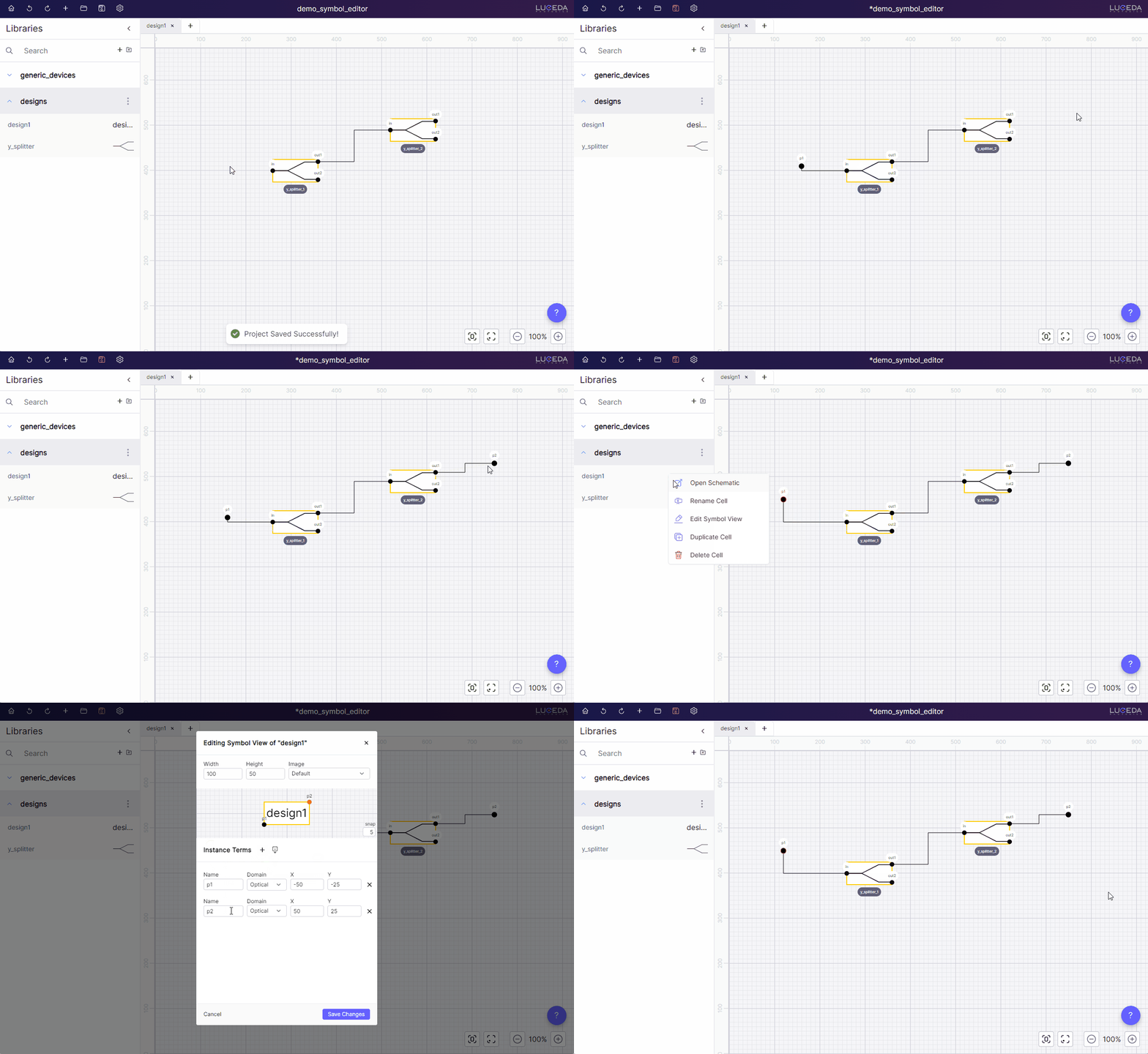
Copy the external terms onto the symbol.