Placement and routing specifications
The advanced placement and routing features of IPKISS can be utilized to design photonic circuits with certain design constraints, such as:
Ensuring minimal spacing of a component relative to another component.
Ensuring waveguides don’t pass through a given part of the layout.
Doing multilayer electrical routing.
When building a layout, sometimes you only know a design constraint (e.g. instance A must be vertically aligned with instance B). Furthermore, it is often easier to provide a relative constraint to a position rather than the absolute coordinate, and you want the tool to resolve these dependencies for you.
IPKISS resolves placement specifications using a constraint solver. This has two advantages: Firstly, in a fully
constrained solution, the order of the specs does not matter. Secondly, by using relative constraints we get a very flexible
and powerful tool for placing our instances. Therefore, we can define certain constraints that will be met regardless of the
parameters of our PCells, using IPKISS placement methods (such as i3.Place, i3.Place.X, i3.Place.Y, i3.Place.Angle, i3.Distribute, i3.Distribute.X and i3.Distribute.Y),
alignment methods (such as i3.AlignH, i3.AlignV), and routing functions (i3.ConnectManhattan, i3.ConnectElectrical).
To help you interpret these specs, we recommend the Luceda Layout Visualizer. It allows you to see a representation of your intent stored in the specs. For now only the connector specs are displayed. This means that you can see which connector is generated by which spec, besides that the control points are also shown.
Introduction
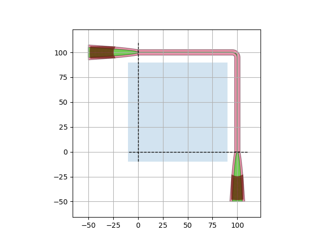
Suppose we have two grating couplers at specific fixed positions with a waveguide connecting them. We would like to construct an MZI underneath it (in the blue area), but it is required by the foundry that waveguides have a minimum spacing of 25 micron between them. The ports of the MZI should also be aligned with the output ports of the grating couplers (see dashed lines).
import si_fab.all as pdk
import ipkiss3.all as i3
import matplotlib.pyplot as plt

min_spacing = 25  # Define a minimum spacing between waveguides

# Instantiate grating couplers and specify the coordinates to place grating coupler outputs
gc = pdk.FC_TE_1550()
X0, Y0, X1, Y1 = 0, 100, 100, 0
specs_basic = [
    i3.Inst(["gc1", "gc2"], gc),
    i3.Place("gc1:out", (X0, Y0)),
    i3.Place("gc2:out", (X1, Y1), angle=90),
    i3.ConnectManhattan("gc1:out", "gc2:out"),
]

circuit = i3.Circuit(specs=specs_basic)
fig = plt.figure()
circuit.Layout().visualize(figure=fig, show=False)

# plot annotations in the figure to mark the relevant constraints
ax = fig.gca()
ax.add_patch(plt.Rectangle((-10, -10), 100, 100, alpha=0.2))
ax.plot((0, 0), (110, -10), (110, -10), (0, 0), color="black", linestyle="--", linewidth=1.0)
plt.show()
Given this layout, we want to place the Y-branches so that their inputs are aligned with the grating couplers in one axis, but that their outputs are at a fixed distance from the waveguide in the other axis. Therefore, the position of the MZI needs to be specified with respect to two separate objects (the grating coupler and the waveguide) at once.
Placement of the MZI
Since the spacing between waveguides can not be lower than 25 microns, the bend_height of the Y-branches are adjusted to conform to this specification.
yb = pdk.YBranch(bend_length=8, bend_height=min_spacing/2)
specs_basic += [i3.Inst(["splitter", "combiner"], yb)]
The MZI can be constructed by specifying the positions of the X and Y coordinates independently. First, the X-coordinate of top Y-branch (splitter) and Y-coordinate of the bottom Y-branch (combiner) are aligned with the grating coupler ports.
specs_basic += [
    # align ports
    i3.AlignV("splitter:in1", "gc1:out"),
    i3.AlignH("combiner:in1", "gc2:out"),
]
Alignment functions such as i3.AlignH and i3.AlignV force the two instances/instance anchors to align along one axis.
If the position of one of the instances/anchors is specified explicitly, the alignment function forces the other instance to match the same
coordinate. In this case, i3.AlignV used to align vertically the input port to the splitter with the output port of the top grating coupler.
Similarly, i3.AlignH is used to align the horizontal coordinates of the combiner and grating ports. The alignment function can also align edges of the bounding boxes
of instances, which can be referenced using symbols. You can learn more about the symbols referencing the bounding boxes of instances in the API reference.
To ensure that the design specs are met, the Y-coordinate of the splitter, and the X-coordinate of the combiner are individually specified with respect to the grating couplers.
specs_basic += [
    # instances, ports, bounding box references @N, @S, @E, @W, @C can be used with placement and routing specs
    # ensure minimum spacing
    i3.Place.Y("splitter:out2", -min_spacing, relative_to="gc1:out"),
    i3.Place.X("combiner:out1", -min_spacing, relative_to="gc2:out"),
    # rotate
    i3.Place.Angle("combiner", 90),
]
i3.Place.X and i3.Place.Y are used to explicitly set the X and Y coordinates of the combiner and the splitter respectively.
Here, the waveguide branch closest to the grating coupler is placed at the minimum spacing away from the grating, which in turn
fixes the final positions of the combiner and splitter. Finally, i3.Place.Angle is used to rotate the combiner.
Since the specs have been defined using relative constraints the conditions will always hold regardless of the parameters of our Y-branches.
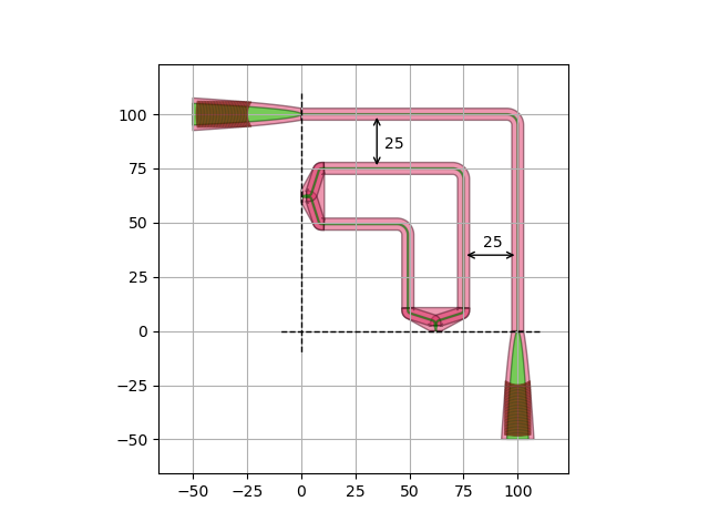
Relative placement of MZI which adheres to design constraints
Let us replace one of the Manhattan routes and add two heater waveguides. Furthermore, since this circuit will have a larger
footprint let’s also increase the distance between the instances, which can be easily done by changing the initial position,
and redefining the specs_basic list. Placement of the heated waveguides can be done implicitly by using i3.Join,
where a port of the heater is overlapped with the port of the splitter/combiner.
X0, Y0, X1, Y1 = 0, 200, 200, 0
specs_basic += [
    i3.Place("gc1:out", (X0, Y0)),
    i3.Place("gc2:out", (X1, Y1), angle=90),
    i3.ConnectManhattan("gc1:out", "gc2:out"),
    # align ports
    i3.AlignV("splitter:in1", "gc1:out"),
    i3.AlignH("combiner:in1", "gc2:out"),
    # ensure minimum spacing
    i3.Place.Y("splitter:out2", -min_spacing, relative_to="gc1:out"),
    i3.Place.X("combiner:out1", -min_spacing, relative_to="gc2:out"),
    # rotate
    i3.Place.Angle("combiner", 90),
    # join the heaters with splitter/combiner
    i3.Join("heater1:in", "splitter:out2"),
    i3.Join("heater2:out", "combiner:out1"),
]
specs = specs_basic + [
    # add connectors, connecting heaters instead
    i3.ConnectManhattan("heater1:out", "heater2:in"),
    i3.ConnectManhattan("splitter:out1", "combiner:out2"),
]

# **syntax is used to unpack and combine all the individual dictionaries
circuit = i3.Circuit(specs=specs)
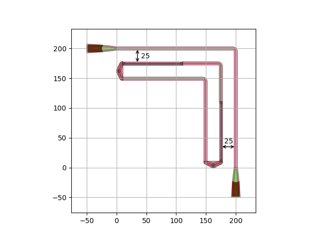
MZI with heaters placed relative to the waveguide, following design constraints
Routing using control points
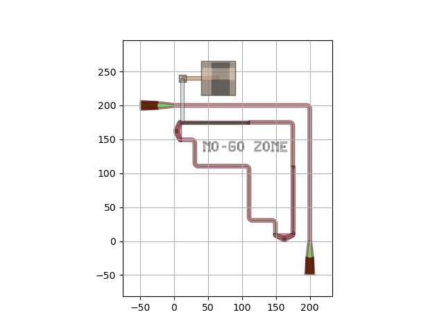
Imagine the situation where the bottom Manhattan route needs to adhere to certain constraints (e.g. it needs to avoid obstacles). We can do this by providing a list of control points to ConnectManhattan. Control points/lines are specific coordinates through which a waveguide is forced to pass. Their location can be explicitly defined, or be specified relative to other instances (including the edges, ports or corners of the instances). They can also be specified relative to the starting/ending/previous control points in your route.
specs = specs_basic + [
    i3.ConnectManhattan(
        "splitter:out1",
        "combiner:out2",
        control_points=[
            i3.V(i3.START + 20),
            i3.H(0, relative_to="heater2:in"),
            i3.V(0, relative_to="heater1@E"),
            i3.H(i3.END + 20),
        ],
    ),
]
i3.V defines a vertical axis, along which the waveguide must pass. Similarly,
i3.H defines a horizontal axis along which the waveguide is routed. i3.START specifies the
‘starting’ coordinates of the waveguide. Therefore, i3.V(i3.START + 20) defines a vertical axis, 20 microns to the east from
the splitter output along which the waveguide must pass.
Note the difference between control points (fixed in both dimensions) and control lines (where a single coordinate is fixed).
To specify the control line using i3.H or i3.V, you can use “anchors”
that define only a single coordinate:
@E and @W specify the x-coordinate/define vertical line,
@N and @S specify the y-coordinate/define horizontal line.
Similarly, control points (with fixed X and Y coordinates) can be specified using i3.CP.
“Anchor points” relative to instances can be used to define such control points.
@C specifies the geometrical center of the instance bounding box,
@NW/@NE/@SW/@SE specify the top-left, top-right, bottom-left, and bottom-right corner of the instance bounding box, respectively.
Custom anchors can also be defined on any cell, which are exposed on instances of this cell. More information can be found here:
i3.Anchor.
More information about the symbols which reference the bounding box of an instance can be found in the API reference.
The Luceda Layout Visualizer can help you interpret the control points and simplifies error resolution.
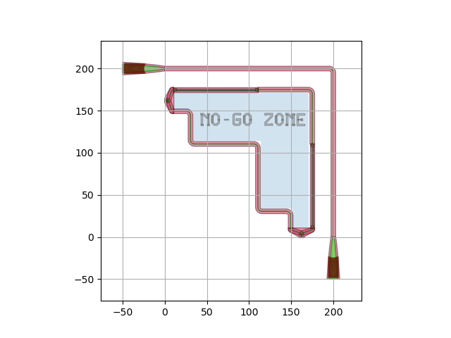
Waveguide routed using control points
S-Bend routing
When two ports are slightly offset but facing the same (or opposite) direction, it might be more space-efficient or geometrically desirable to connect them using an S-Bend rather than a Manhattan route. The i3.ConnectSBend specification provides an easy way to generate an S-Bend between two ports.
You can customize the S-Bend by specifying the min_bend_radius, trace_template, and bend_type (e.g. i3.SBendType.Sine or i3.SBendType.Euler). The specified min_bend_radius is strictly enforced and an error is raised when violated.
import si_fab.all as pdk
import ipkiss3.all as i3

circuit = i3.Circuit(
    specs=[
        i3.Inst(["wg1", "wg2"], pdk.Waveguide()),
        i3.Place("wg1", (0.0, 0.0)),
        i3.Place("wg2", (50.0, 20.0)),
        i3.ConnectSBend("wg1:out", "wg2:in", sbend_type=i3.SBendType.Sine, min_bend_radius=10.0),
    ],
)
circuit.Layout().visualize()
Electrical routing
As a last step, let’s connect one of the heaters to a bondpad.
We shall utilize the multilayer electrical routing to route the even metal layers in the vertical direction
and odd metal layers in the horizontal direction.
You might want to do this when you want to guarantee an easy escape route in the electrical domain out of your
circuit.
This can be done by defining a VIA array that we’ll be using when defining i3.VIA(s) as control points in
i3.ConnectElectrical.
The absolute coordinates of the Bondpad (pad) are specified using i3.Place.
We use VIAs to move between different metal layers and define the path of the electrical routes.
To control where the VIAs are placed, we make use of the relative_to argument (same as in i3.CP/i3.H/i3.V).
Our goal is to have the minimal length Manhattan-like route, which can be achieved by placing
VIAs relative to the bondpad center and the electrical ports of the heaters.
Placement relative to the two objects is done using the following statement i3.VIA((-1.5, 0), relative_to=("heater1@E", "pad@C")).
The small addition compensates for half of the width of the electrical ports. Note that the relative_to argument supports “anchors” referring to two different instances,
which we readily use.
Finally, at the point where we place the VIA we also switch the metal trace, which ensures correct traces are used in each of the routing directions.
specs += [
    # adding bondpad
    i3.Place("pad@C", (dx, 1.2 * Y0)),
    # Use multiple vias in Electrical route
    i3.ConnectElectrical(
        "heater1:elec1",
        "pad:m1",
        trace_template=M2_wire_tpl,
        start_angle=90,
        end_angle=180,
        control_points=[
            i3.VIA(
                (0, 0),
                relative_to=("heater1:elec1", "pad@C"),
                direction_in=i3.SOUTH,
                direction_out=i3.EAST,
                trace_template=M1_wire_tpl,
                layout=via_array,
            ),
        ],
    ),
]
Electrical routing using IPKISS placement and routing functions
For more details on placement and routing, or on particular specification, see the Placement and Routing API reference.