Introduction
Arrayed waveguide grating
An arrayed waveguide grating (AWG) is a planar optical filter device which can process a range of optical channels at once. The most common applications for AWGs are as a multiplexer or demultiplexer device, or as an element in switches (e.g. crossbar). Since they can also influence the phase of the signals, they are sometimes used in dispersion compensation applications as well. Besides their use in telecom and datacom networks, they can also be employed in spectrometer devices, such as in medical sensing (e.g optical coherence tomography) or in mechanical sensing (e.g. fiber Bragg grating read-out).
AWGs have many parameters and offer a relatively large degree of freedom, though many parameters are coupled, leading to multiple design trade-offs. By using the Luceda AWG Designer module, some of this complexity is removed by means of design automation, while keeping the flexibility to tailor the AWG design where needed.
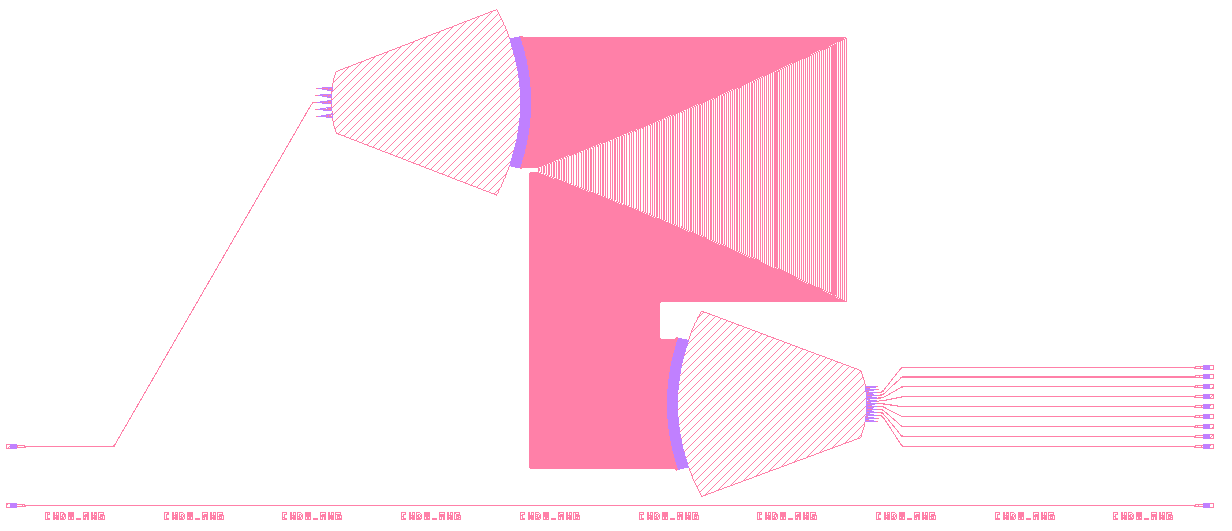
An AWG consists of input/output waveguides, star couplers and a waveguide array connecting them.
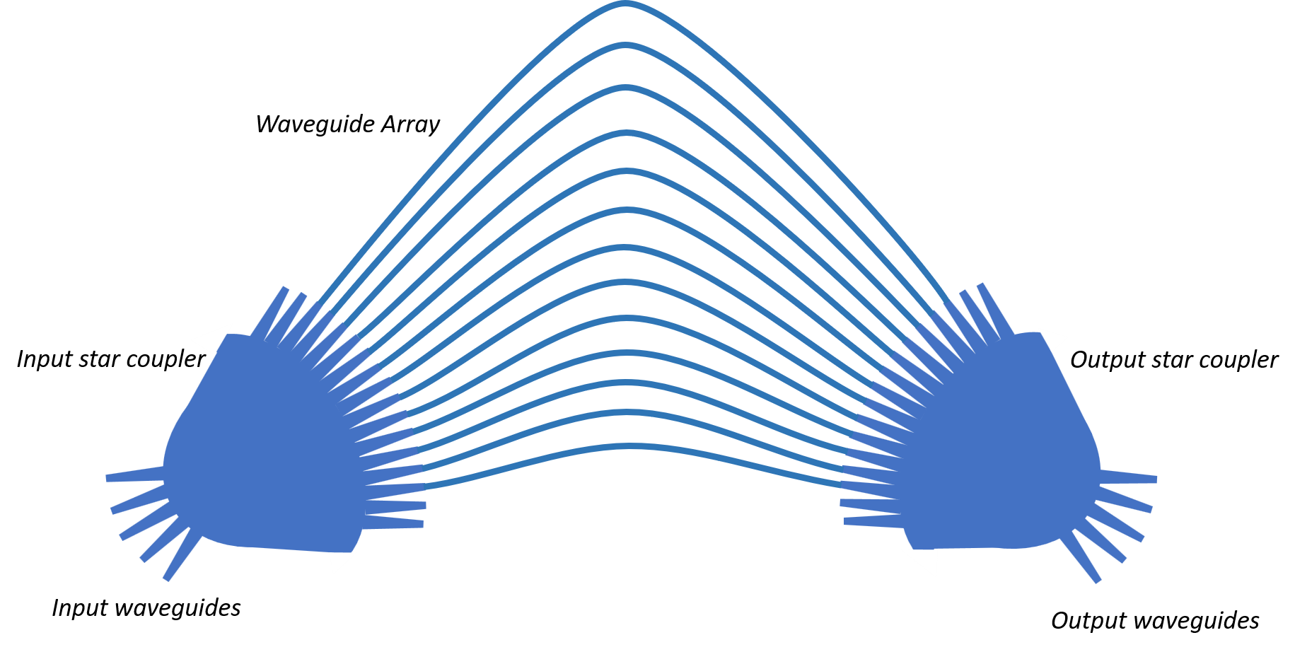
The working principle of an AWG is simple. Light entering the first star coupler through the input waveguide is diffracted and coupled into the waveguide array with a specific phase difference between two successive arms. If we place the output waveguides at the right positions, wavelength channels can be demultiplexed into the various output waveguides.
Specification-driven workflow
The overall concept of using the Luceda AWG Designer is as follows:
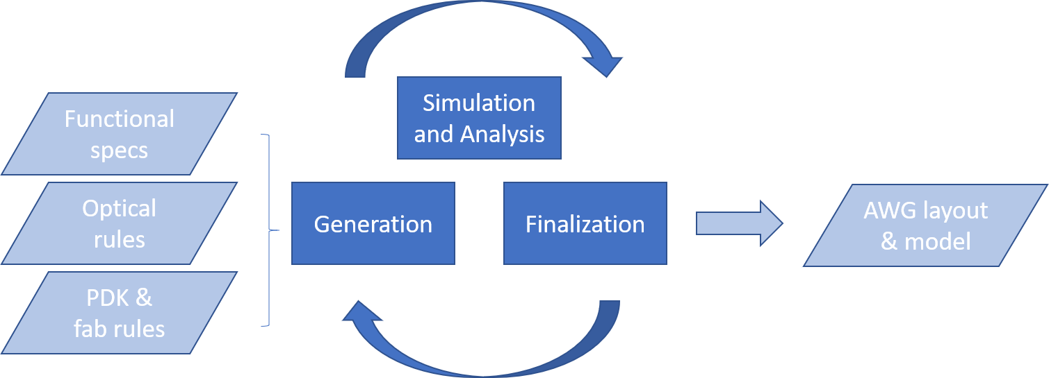
The input consists of functional specifications, optical rules, and PDK and fab rules. The output of the design flow is a finished AWG with a reusable layout and a circuit model.
In this tutorial we will go through all the design steps of an AWG:
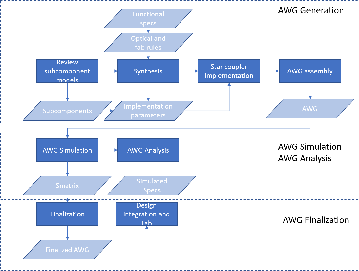
AWG generation
First, the subcomponents (slab template, apertures and waveguide model) need to be designed.
Then, based on functional specifications and fab and optical rules, the AWGs are generated and implementation parameters, such as angles, positions, radii, delay length, are derived.
Finally, the AWG is assembled based on these implementation parameters: first the star couplers and then the full AWG.
AWG simulation and analysis. In this step, the entire AWG is simulated from first principles. The results of the simulation are analyzed and high-level specs such as cross-talk or insertion loss are calculated.
AWG finalization. Finally, the AWG design is finalized so that it can be easily integrated with the rest of the circuit, e.g. routing of its inputs and outputs to Manhattan directions, and saving the AWG layout and model for subsequent use within the Luceda Photonics Design Platform.
Application: 400G Ethernet
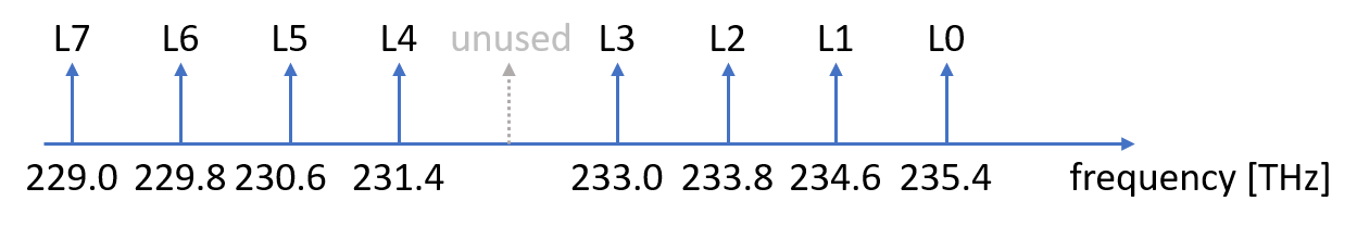
In this tutorial, we target a data communication application, specifically 400GBase-LR8 [3]. However, the design flow and principles can be equally applied to other applications as well. 400GBase-LR8 is an IEEE physical layer standard for 400 Gbit/s Ethernet over 10km or further. It uses 8 parallel wavelength channels with a coarse spacing (CWDM) at 50 Gbit/s each.
In the transmitter optical sub-assembly (TOSA) and receiver optical sub-assembly (ROSA) for such a system, 8-channel multiplexing (mux) and demultiplexing (demux) components are needed, respectively. The channels are coarsely spaced across the O-band (1260-1360 nm), using a step of 800 GHz around a center frequency of 232.2 THz. The center frequency itself is unused. In this tutorial, we will design an AWG so that it meets these specifications and we will prepare it for tape-out and further re-use within a circuit design.
Lane |
Center frequency (THz) |
Center wavelength (nm) |
Wavelength range |
|---|---|---|---|
L0 |
235.4 |
1273.55 |
1272.55 to 1274.54 |
L1 |
234.6 |
1277.89 |
1276.89 to 1278.89 |
L2 |
233.8 |
1282.26 |
1281.25 to 1283.28 |
L3 |
233.0 |
1286.66 |
1285.65 to 1287.69 |
L4 |
231.4 |
1295.56 |
1294.53 to 1296.59 |
L5 |
230.6 |
1300.05 |
1299.02 to 1301.09 |
L6 |
229.8 |
1304.58 |
1303.54 to 1305.63 |
L7 |
229.0 |
1309.14 |
1308.09 to 1310.19 |
Design project structure
To guide you through the structure of this tutorial, we have created four custom functions:
generate_awg: it executes all the steps for the AWG generation and it returns an AWG PCell.simulate_awg: it takes the generated AWG PCell as an input, simulates it and returns its S-matrix.analyze_awg: it takes an S-matrix as an input, performs the analysis and returns a report on the specifications.finalize_awg: it takes an AWG PCell as an input and returns a routed and fab-ready AWG in GDSII format.
These functions have been custom-written for this example. It is recommended that each designer creates their own functions, customizing them and choosing the desired parameters that need to be varied.
The code below goes through all these steps.
The results are stored in the folder designs/awg_10400_0.4, which contains:
The finalized GDSII file of the AWG
The simulated spectrum
An analysis report
import si_fab.all as pdk  # noqa: F401
import ipkiss3.all as i3
import numpy as np
import os

from rect_awg.generate import generate_awg
from rect_awg.simulate import simulate_awg
from rect_awg.finalize import finalize_awg
from rect_awg.analyze import analyze_awg

# Actions
generate = True
simulate = True
analyze = True
finalize = True
plot = True

# Specifications
wg_width = 0.4
fsr = 10400

# Creating a folder for results
this_dir = os.path.abspath(os.path.dirname(__file__))
designs_dir = os.path.join(this_dir, "designs")
if not os.path.exists(designs_dir):
    os.mkdir(designs_dir)
save_dir = os.path.join(designs_dir, "awg_{}_{:.1f}".format(fsr, wg_width))
if not os.path.exists(save_dir):
    os.mkdir(save_dir)

# Simulation specs
wavelengths = np.linspace(1.26, 1.32, 1000)

# Bare AWG
if generate:
    awg = generate_awg(fsr=fsr, wg_width=wg_width, plot=plot, save_dir=save_dir, tag="bare")
if simulate:
    smat = simulate_awg(awg=awg, wavelengths=wavelengths, save_dir=save_dir, tag="bare")
else:
    path = os.path.join(save_dir, "smatrix_bare.s10p")
    smat = i3.device_sim.SMatrix1DSweep.from_touchstone(path, unit="um") if os.path.exists(path) else None

if analyze:
    analyze_awg(smat, plot=True, save_dir=save_dir, tag="bare")

# Finished AWG
if finalize:
    if generate:
        finalized_awg = finalize_awg(awg=awg, plot=plot, save_dir=save_dir, tag="finalized")

    if simulate:
        smat_finalized = simulate_awg(
            awg=finalized_awg.blocks[3],
            wavelengths=wavelengths,
            save_dir=save_dir,
            tag="finalized",
        )
    else:
        path = os.path.join(save_dir, "smatrix_finalized.s10p")
        smat_finalized = i3.device_sim.SMatrix1DSweep.from_touchstone(path, unit="um") if os.path.exists(path) else None

    if analyze:
        analyze_awg(smat_finalized, peak_threshold=-25, plot=plot, save_dir=save_dir, tag="finalized")

print("Done")
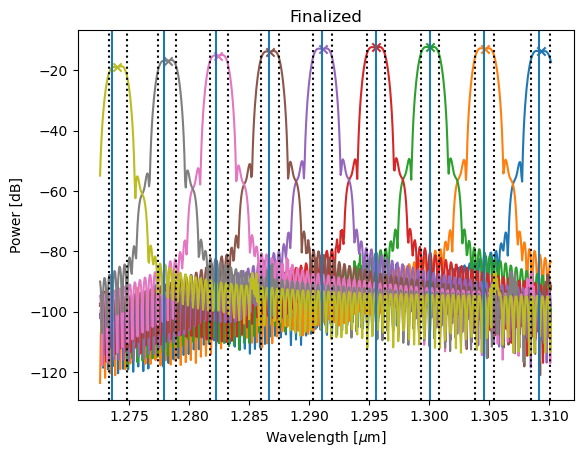
Analysis report: report_finalized.json
Conclusion
The AWG Designer module consolidates all steps of the design process and produces a manufacturable AWG, as well as matching simulation results and analysis reports. A code structure is proposed that matches well the four design steps:
AWG generation
AWG simulation
AWG analysis
AWG finalization
Test your knowledge
In order to become familiar with the design procedure please run the following file:
luceda-academy/training/topical_training/cwdm_awg/example_generate_awg.py
As an exercise, try to change the FSR of the AWG to 12000 GHz and compare the result with the 10400 GHz.
Has the insertion loss increased or decreased?
Has the crosstalk increased or decreased?