AWG finalization
In the previous step, we implemented the AWG device starting from the derived implementation parameters. Now, we still need to make sure the AWG can be used in a larger circuit and is ready for tape-out. For instance, many fabs impose design rules to avoid acute (sharp) angles. In order to test the AWG, we will also include it in a small test design.
All of these steps are performed in the finalize_awg function, defined in rect_awg/finalize.py, that takes an AWG PCell as input and returns a routed AWG that can be merged in a top-level layout.
Let’s have a look at the function signature.
def finalize_awg(awg, plot=True, die_width=3000.0, save_dir=None, tag=""):
    """Custom function to finalize an AWG design, mostly for DRC fixing and routing.
    If you make an AWG, you should write one of your own.
    Parameters are the things you want to vary as well as options to control whether you
    plot and where you save your data.

    Parameters
    ----------
    awg: i3.PCell
         Input AWG cell
    plot : bool, default: True, optional
           If true the finilized awg is plotted
    die_width: float, default: 3000.0, optional
               Width of the die
    save_dir : str, default: None, optional
               If specified, a GDSII file is saved in this directory
    tag: str, optional
         String used to give a name to saved files

    Returns
    -------
    awg_block: i3.PCell
               Finalized AWG block
    """
Preparing for tape-out
To prepare the AWG for tape-out and make it adhere to design rules, we need to do some small changes to the layout.
This involves three activities:
Fine-tuning the drawing of the star coupler contour
Patching acute angles (by adding stubs)
Flattening the full design to avoid snapping errors, caused by the rotation of subcell instances
Typically, making DRC-clean layouts is very foundry-specific. Therefore, Luceda IPKISS provides functionality to make the task easier:
Detection of acute angles in the layout
Stubbing of acute angles
Merging shapes on the same layer and other boolean operations
A list of these operations can be found in the documentation: layout operations.
Star coupler contour
The contour of the star coupler is drawn using the get_star_coupler_extended_contour function.
Please check the Luceda AWG Designer documentation to learn about all the parameters that can be changed.
For this example, we used the following parameters:
contour = awgd.get_star_coupler_extended_contour(
    apertures_in=sc_in_ports,
    apertures_out=sc_in_array,
    trans_in=sc_in_ports_xforms,
    trans_out=sc_in_array_xforms,
    radius_in=grating_radius_input*0.5,
    radius_out=grating_radius_input,
    extension_angles=(10, 10),
    aperture_extension=(1.0, 0.0),
    layers_in=[i3.TECH.PPLAYER.SI],
    layers_out=[i3.TECH.PPLAYER.SI],
)
Let’s have a closer look at some of these parameters:
The
aperture_extensionsparameter, if nonzero, determines whether we draw extra points along the front shape of the aperture at a certain distance. When a layer is given, this layer is matched against a waveguide window to determine the width of the window. In this example, we look for the width of the coreSIlayer (layer), and extend it with 1 \(\mu m\) on the input side, and 0 \(\mu m\) on the output side.Using the parameter
extension_angleswe decide how far outwards the contour is drawn: we extend the contour region with 10 degrees on the input side, and 10 degrees on the output side.
As a result we obtain a contour which matches the apertures exactly and avoids acute angles:
Patching acute angles by adding stubs
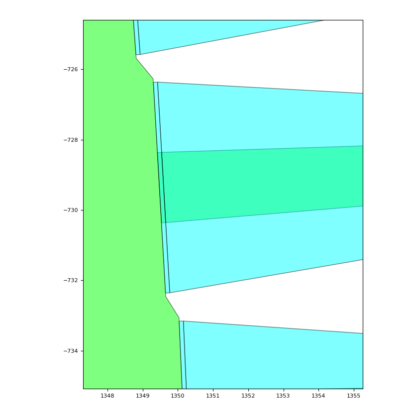
One obvious design rule violation happens when two apertures are close together and the SHALLOW layer creates acute (sharp) angles (indicated by the arrows on the image below).
Acute angles in the SHALLOW layer of an aperture array.
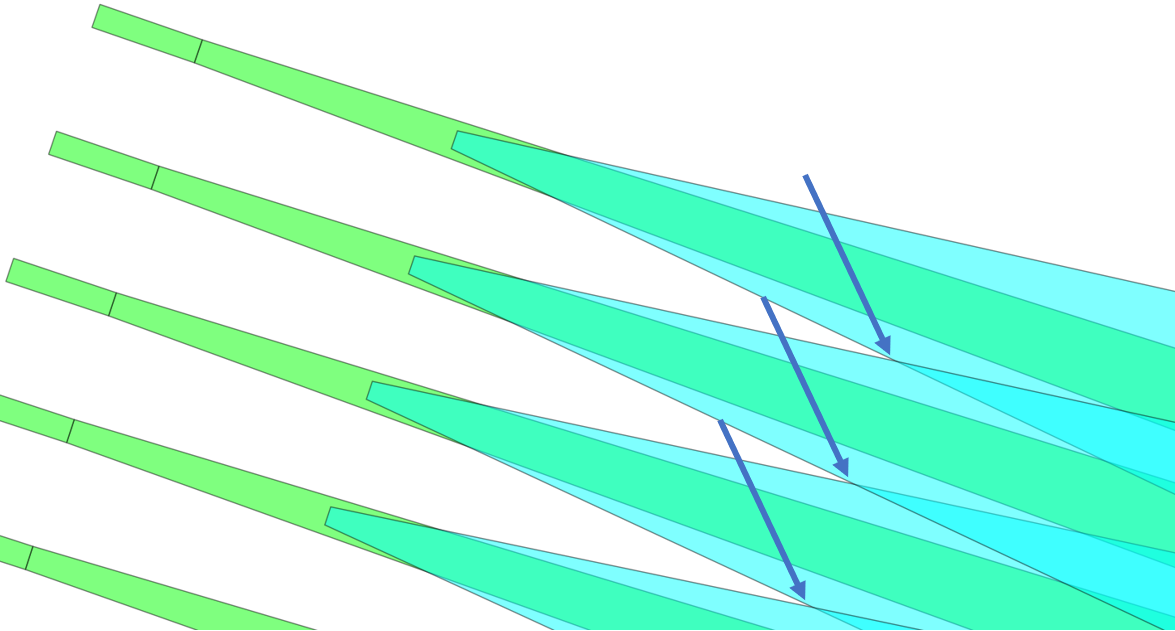
To fix those errors, we can use Luceda IPKISS’ method i3.get_stub_elements.
This function takes a layout as input and returns two lists of elements, elems_add and elems_subst, that we can use to add and subtract, respectively, from the layout.
elems_add, elems_subt = i3.get_stub_elements(
    awg_layout,
    angle_threshold=0,
    layers=[i3.TECH.PPLAYER.SHALLOW],
    grow_amount=0.001,
)
After the stubbing operation, the corrected apertures would look like this (note that we will apply the patches only in a later stage, this is only for illustration purposes):
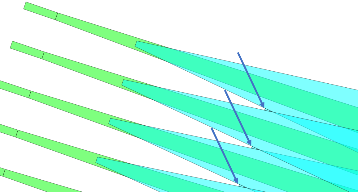
Stubbing acute angles in the aperture array.
Flattening the AWG
Currently, our AWG consists of three instances, the input star coupler, the waveguide array, and the output star coupler. Each instance has a certain transformation applied in order to connect them together. Certainly, when there are non-orthogonal angles in these transformations or any of the underlying transformations, it is impossible to get a perfect alignment of two ports that are supposed to be connected. To solve this, we need to flatten the AWG.
On the other hand, we want to keep the netlist and model of the AWG intact, as we intend to use this for running circuit simulations. For that reason we create a new cell in which we’ll add all the information (flattened layout, but original netlist and model):
    # Wrap in a cell with a clean layout
    awg_clean_layout = awg_layout.layout.flat_copy() + elems_add
    awg_clean = i3.EmptyCell(name="awg_clean")
    awg_clean.Layout(layout=awg_clean_layout, ports=awg_layout.ports)
    awg_clean.Netlist(terms=awg_netlist.terms)
    awg_clean.CircuitModel(model=awg_circuit.model)
    ports = [p for p in awg_layout.ports if "out" in p.name]
Note
Each design might require a slightly different approach to make the AWGs fully DRC clean. For more information on methods that help create DRC-clean layouts, you can check the Luceda IPKISS API reference: layout operations.
Using the AWG in a chip
Final layout
As a final step of this tutorial, we will prepare a test structure on a real chip so we can test the AWG. To do so, we will go through the following steps:
We will fan out the waveguides and route them to fiber grating couplers for testing.
An alignment waveguide will be added, for easier alignment of the fibers and normalizing the transmission spectrum of the AWG.
We will add some text labels on the chip so that we can easily recognize it under the microscope.
And finally, we’ll also add a company logo - that is going to look nice when taking pictures.
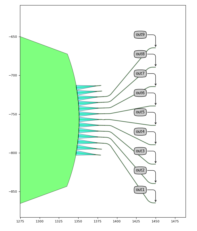
Currently, the AWG ports are still on irregular angles and pitch.
Routing them to Manhattan directions and on a regular pitch can easily be done with FanoutPorts:
    # Fanout ports to horizontal on a regular pitch
    wg_tmpl = pdk.SiWireWaveguideTemplate()
    wg_tmpl.Layout(core_width=0.4)

    y_spacing = 25.0
    awg_routed = FanoutPorts(
        name="routed_awg",
        contents=awg_clean,
        trace_template=wg_tmpl,
        port_labels=["E" + str(cnt) for cnt in range(len(ports))],
    )
    awg_routed_layout = awg_routed.Layout(
        bend_radius=10.0,
        target_coordinate=1450.0,
        spacing=y_spacing,
        reference_coordinate=awg_layout.ports["out4"].y - 4 * y_spacing,
    )
By playing a bit with the parameters we can obtain the desired layout.
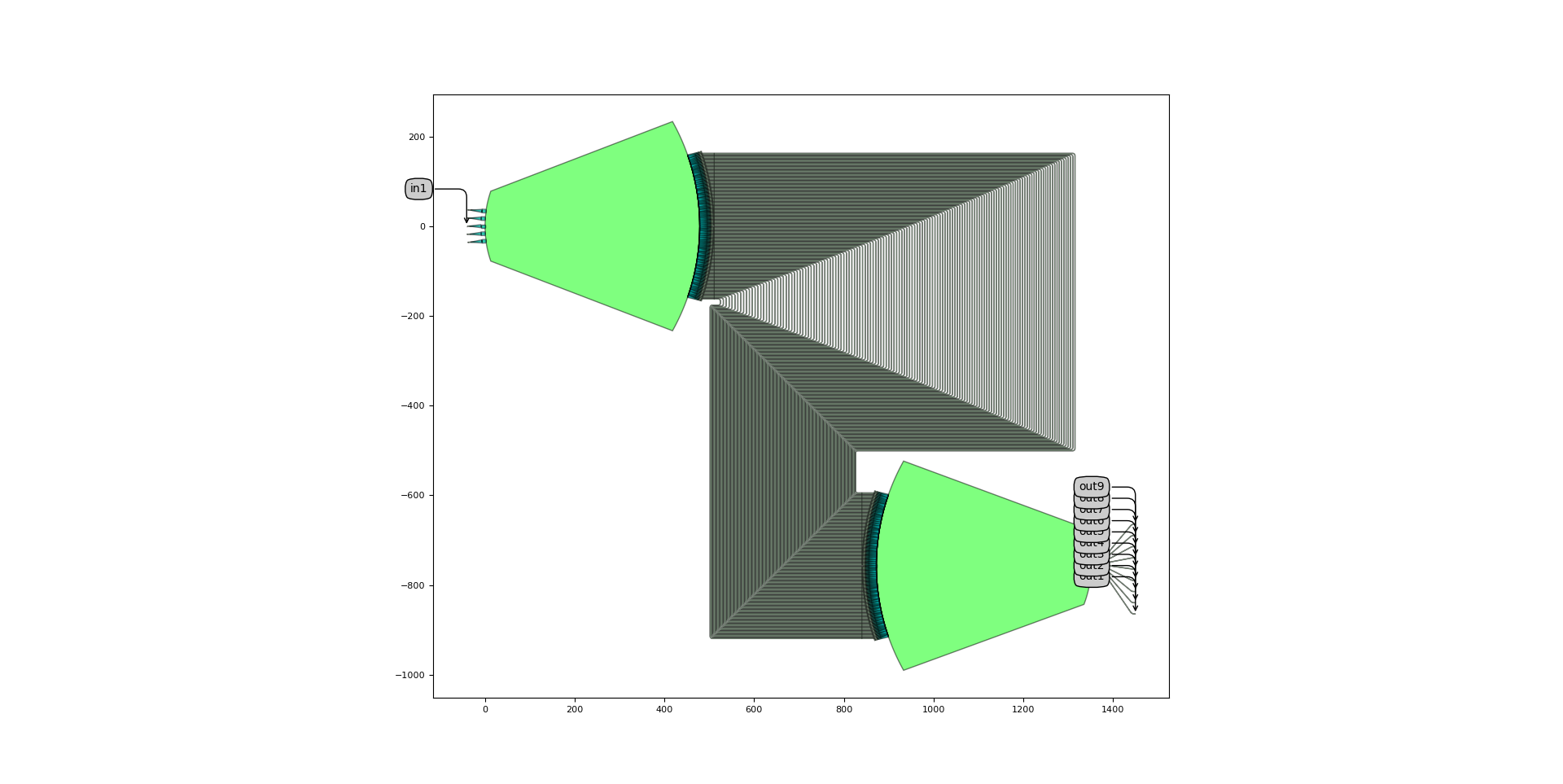
Luceda IPKISS also provides functionality for adding grating couplers and other structures required to make a test structure.
The IoColumn class allows us to attach cells to the grating couplers, add alignment waveguides, text labels and more.
    # Define fiber coupler adapter
    class IoFibcoup1300(IoFibcoup):
        def _default_trace_template(self):
            return wg_tmpl

        def _default_fiber_coupler(self):
            return pdk.FC_TE_1300()

    # Make an AWG test structure
    print("Making AWG test structure...\n")
    awg_block = i3.IoColumn(name="awg_test", adapter=IoFibcoup1300)
    awg_block_layout = awg_block.Layout(south_east=(die_width, 0.0), y_spacing=25.0)
    awg_block.add_blocktitle("CWDM_AWG")
    awg_block.add_align(trace_template=wg_tmpl)
    awg_block.add_emptyline(8)
    awg_block.add(
        awg_routed,
        relative_offset=(0.0, awg_routed_layout.ports["in1"].y - awg_routed_layout.ports["out1"].y),
    )
Let’s have a closer look at this code:
First, we define the adapter
IoFibcoupto be used, which adds tapers and fiber couplers automatically.We make an
IoColumn, which is a kind of block to which we can add devices under test as well as fiducials. TheIoColumnis made 3 mm-wide by setting itssouth_eastcorner (south-west being the origin). We set the fiber coupler pitch to 25 um and the adapter to the one we just defined.Next, we add a title which will be repeated along the width of the block, defined in
die_width.Then, an alignment waveguide is added.
Finally, the AWG is added. In order to position it nicely, we add a few empty lines (of 5 um x 25 um pitch) and a vertical offset to the AWG. Obtaining the right parameters requires a little bit of playing around, but
IoFibcoupprovides a lot of flexibility.
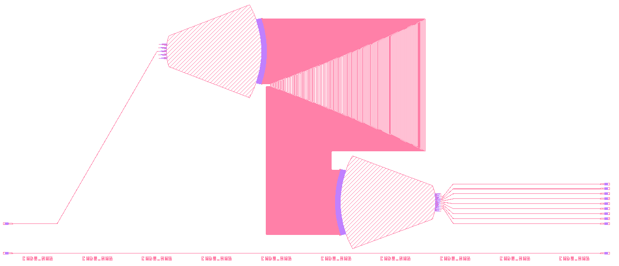
As a result, we obtain the following layout:
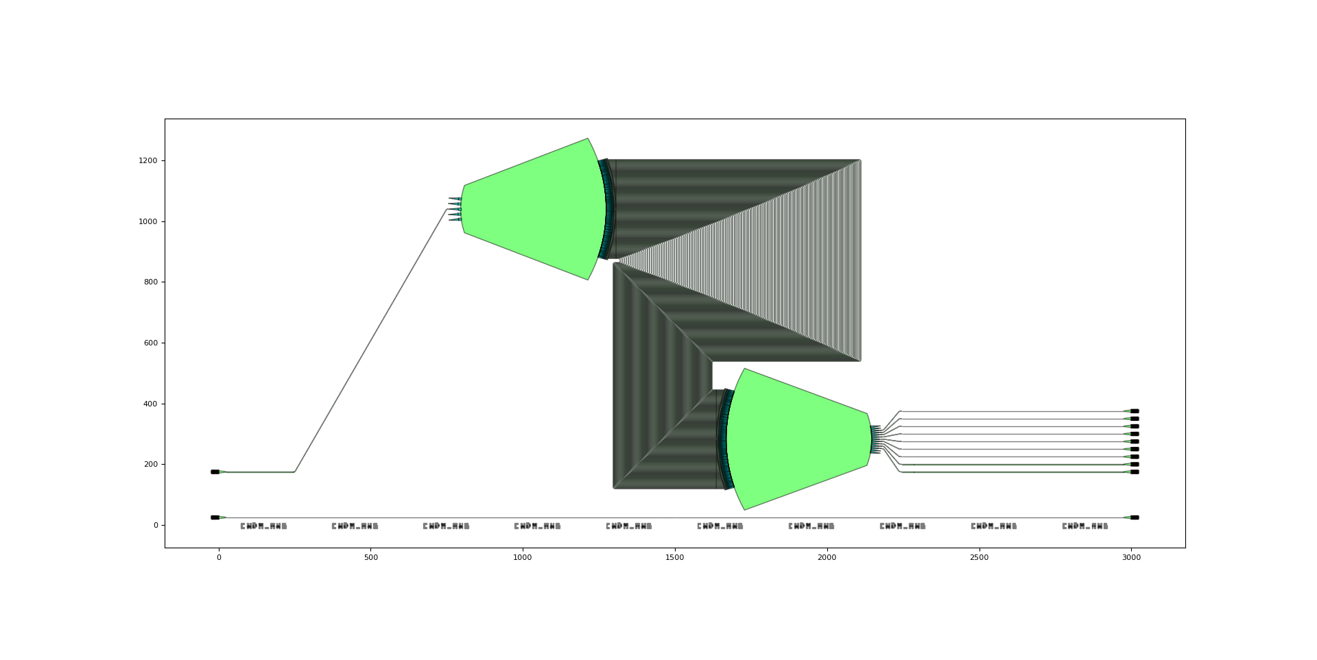
Ultimately, we obtain our finalized layout, ready to be incorporated on a test maskset:
Final simulation and analysis
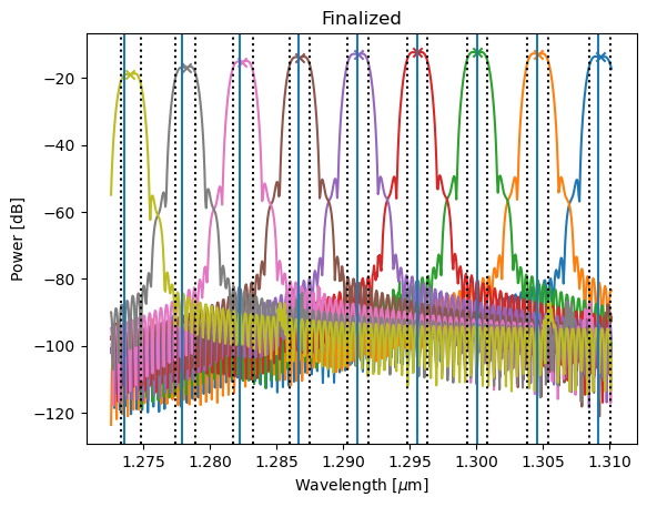
Now we can simulate the transmission of the devices on the chip to check that our test structures allow us to extract the information we need about the device under test (the AWG in this case).
The alignment waveguide is the second object we added to the block (index 1) and the AWG is the fourth (index 3).
We retrieve their circuit models from which we simulate the spectra
All effects in the devices under test are taken into account, including the waveguide losses and the performance of the fiber grating couplers.
In addition, we can use the previously defined simulate_awg and analyze_awg functions to analyze the S-matrix of the AWG, including the behavior from the fiber grating couplers.
Since the transmitted power has considerably dropped due to the fiber grating couplers, we set the threshold for peak detection to -25 dB.
# Finished AWG
if finalize:
    if generate:
        finalized_awg = finalize_awg(awg=awg, plot=plot, save_dir=save_dir, tag="finalized")

    if simulate:
        smat_finalized = simulate_awg(
            awg=finalized_awg.blocks[3],
            wavelengths=wavelengths,
            save_dir=save_dir,
            tag="finalized",
        )
    else:
        path = os.path.join(save_dir, "smatrix_finalized.s10p")
        smat_finalized = i3.device_sim.SMatrix1DSweep.from_touchstone(path, unit="um") if os.path.exists(path) else None

    if analyze:
        analyze_awg(smat_finalized, peak_threshold=-25, plot=plot, save_dir=save_dir, tag="finalized")

print("Done")
Report JSON file: report_finalized.json
We can clearly see the fiber coupler spectrum overlayed (twice, for the input and the output coupler) on the alignment waveguide and the AWG. The spectrum of the AWG test structure can then be normalized to the one of the alignment waveguide to get a relatively accurate estimate of the transmission of the AWG itself.
Conclusion
In this final part of the tutorial, we made sure that the AWG adheres to layout design rules, and we’ve routed the AWG to the outside world to obtain a design ready for tape-out. Finally, a test structure was created and validated in simulation for testing and extracting the AWG performance.
Test your knowledge
Create an AWG sweep to understand the effect of a parameter on the performance.
Make a copy of
luceda-academy/training/topical_training/cwdm_awg/example_generate_awg.py(e.g. generate_awg2.py)Make a copy of the
rect_awgfolder (including the functions inside) (e.g. rect_awg2)Make sure to update the import statements in
generate_awg2.pyto use the functions defined inrect_awg2.Now you can change anything about the design. Using a
forloop you can define a parameter sweep.
Try to sweep the following parameters:
Number of arms in the AWG
Length of the MMI aperture in the AWG
FSR of the AWG
Output spacing
Doing so will allow you to emulate the typical flow you will go through when designing your AWGs, as you will want to check what the effect of certain parameters is on your spec. Most likely, several designs will be included in your final mask.