AWG generation: Subcomponents
In order to design and implement an AWG, we need a few basic aspects and components:
The material models, which will be used to simulate modes and fields
The slab template, which specifies the cross-section information for the free propagation region
The apertures, which feed light in and out of the star couplers
The waveguides and waveguide model which will form the waveguide array

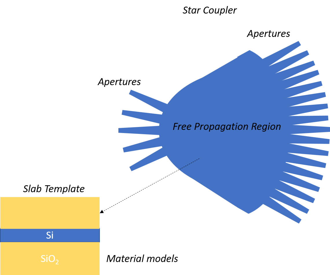
For each of these components, we need to ensure the parameters are matching our technology and application. Once we control these, we can design an AWG and define its input and output star couplers and its waveguide array. The simulation of AWGs by the AWG Designer is performed using a hierarchical model, which builds up a model of the complete AWG by taking the models of its subcomponents, starting from the material models.
Materials
The material models (real part n and imaginary part k of the refractive index) are used to calculate slab waveguide modes (slab template) and aperture waveguide modes. Therefore, we need to ensure that the correct material model as a function of wavelength is used.
Every Luceda PDK contains material models. In this tutorial, we are using the SiFab PDK, which contains silicon and silicon dioxide material models. Each optical material has a get_epsilon() method which we can use to check its relative permittivity as a function of wavelength, as illustrated in the code below.
import si_fab.all as pdk  # noqa: F401
import ipkiss3.all as i3
import numpy as np
import pylab as plt

TECH = i3.get_technology()

wavelengths = np.linspace(1.25, 1.35, 100)

epsilon_si = [
    TECH.MATERIALS.SILICON.get_epsilon(
        i3.Environment(
            wavelength=wavelength,
        ),
    ).real
    for wavelength in wavelengths
]

epsilon_sio2 = [
    TECH.MATERIALS.SILICON_OXIDE.get_epsilon(
        i3.Environment(
            wavelength=wavelength,
        ),
    ).real
    for wavelength in wavelengths
]

plt.subplot(211)
plt.plot(wavelengths, epsilon_si, "b-", linewidth=5)
plt.xlabel("Wavelength [um]")
plt.ylabel(r"$\epsilon_r$")
plt.title("Relative permittivity of silicon")
plt.subplot(212)
plt.plot(wavelengths, epsilon_sio2, "b-", linewidth=5)
plt.xlabel("Wavelength [um]")
plt.ylabel(r"$\epsilon_r$")
plt.title(r"Relative permittivity of SiO2")
plt.tight_layout()
plt.show()
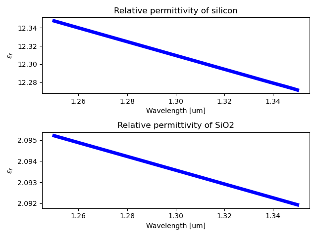
Behind the scenes, AWG Designer uses ‘get_epsilon()’ to calculate the permittivity distribution of the slabs and apertures and thus calculate the modes of the slabs and the propagation through the apertures. It is thus important to make sure that these values are correct in the wavelength range for which you are designing your AWG. If you are creating your own PDK, you would need to implement your own material models. This is to make sure that the design created for your PDK, and the outcome of simulations, are both correct.
Test your knowledge
Open plot_material.py and run it to visualize the material models in the SiFab PDK.
Is this the behaviour you would expect from silicon and silicon dioxide?
File location: luceda-academy/training/topical_training/cwdm_awg/components/plot_material.py
Slab template
The template si_fab_awg.all.SiSlabTemplate describes the cross-section and modes of the SOI slab waveguide.
It is implemented in si_fab, in the si_fab_awg module.
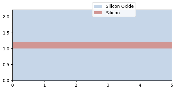
We can visualize its properties to ensure correctness. The cross-section can be obtained from its layout view:
import si_fab.all as pdk  # noqa: F401
from si_fab_awg.all import SiSlabTemplate
import numpy as np

# Instantiate slab
slab = SiSlabTemplate()

# Visualize cross-section
slab_layout = slab.Layout()
slab_xs = slab_layout.cross_section()
slab_xs.visualize()
The slab waveguide’s modes are obtained automatically by running a CAMFR simulation on the cross-section. Two inputs are essential:
The wavelength range within which we calculate the modes. Here, we select the band between 1.25 um and 1.35 um.
The material models, verified in the previous step.
The resulting mode effective indices can be plotted and checked easily:
# Calculate and visualize modes
wavelengths = np.linspace(1.25, 1.35, 101)
slab_modes = slab.SlabModesFromCamfr(wavelengths=wavelengths)
slab_modes.visualize(wavelengths=wavelengths)
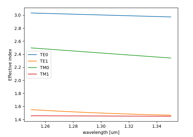
In AWG Designer, the slab modes are used in simulating light propagation through the free-propagation region of the star couplers (see this tutorial on the simulation of AWGs).
Test your knowledge
Open plot_slab.py and run it to visualize the guided modes of the SOI slab waveguide.
Is this the behaviour you would expect?
Why is the effective index for TM0 lower than the one for TE0?
File location: luceda-academy/training/topical_training/cwdm_awg/components/plot_slab.py
Waveguide aperture
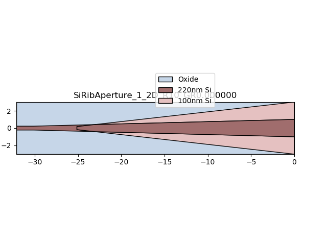
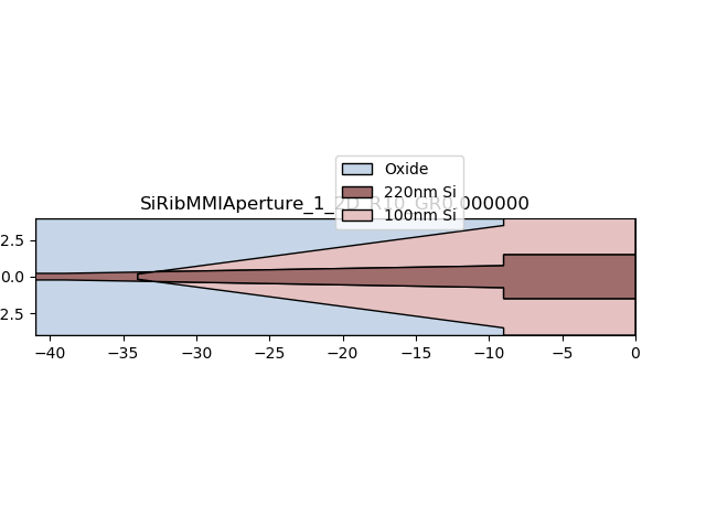
In order to couple light efficiently into and out of the star coupler with low reflection or scattering, we will use a rib waveguide with partially etched silicon.
The si_fab_awg module contains si_fab_awg.all.SiRibAperture which transitions from a single-mode fully etched strip waveguide to a broader (multimode) rib waveguide and finally into the SOI slab waveguide characterized by the si_fab_awg.all.SiSlabTemplate.
It is important to explicitly define which slab template the aperture opens into, and in particular the wavelength range of the slab’s model:
import si_fab.all as pdk # noqa: F401
from si_fab_awg.all import SiSlabTemplate, SiRibAperture
import ipkiss3.all as i3
import numpy as np
wavelengths = np.linspace(1.25, 1.35, 100)
center_wavelength = 1.3
slab_tmpl = SiSlabTemplate()
slab_tmpl.SlabModesFromCamfr(wavelengths=wavelengths)
aperture = SiRibAperture(
slab_template=slab_tmpl,
taper_length=30.0,
aperture_core_width=2.0,
wire_width=0.4,
)
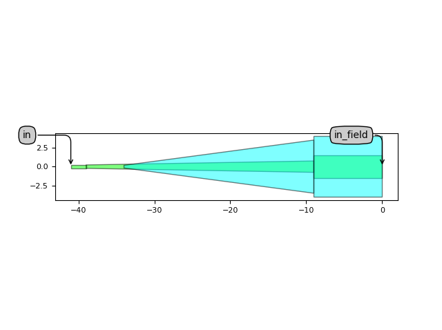
# Layout
print("Instantiating aperture layout...\n")
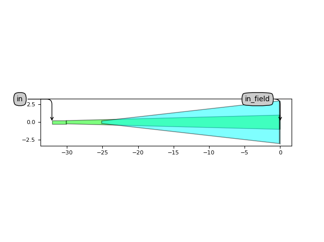
aperture_lay = aperture.Layout()
aperture_lay.visualize(annotate=True)
aperture_lay.visualize_2d(process_flow=i3.TECH.VFABRICATION.PROCESS_FLOW_FEOL)
The aperture is then simulated, by default, using CAMFR. The field profile at the aperture opening is then obtained from the CAMFR simulation.
The slab template is used by the aperture in two ways:
The field profile at the aperture opening is decomposed in terms the modes of the slab template
The far field is calculated using the properties of the slab modes
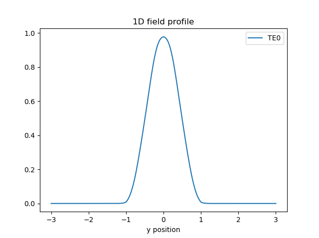
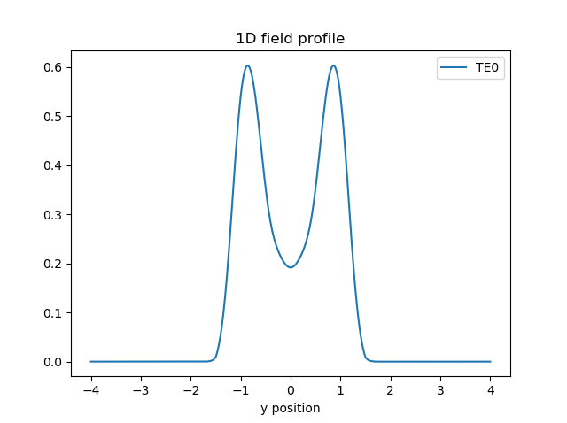
First, let’s check the output field at the aperture into the slab. In this case, it is calculated automatically using CAMFR, similarly to Multi-mode interferometer (MMI).
# Field model
fieldmodel = aperture.FieldModelFromCamfr()
env = i3.Environment(wavelength=center_wavelength)

# Field profile at the aperture
print("Simulating field profile at aperture...\n")
fields = fieldmodel.get_fields(mode=0, environment=env)
fields.visualize()
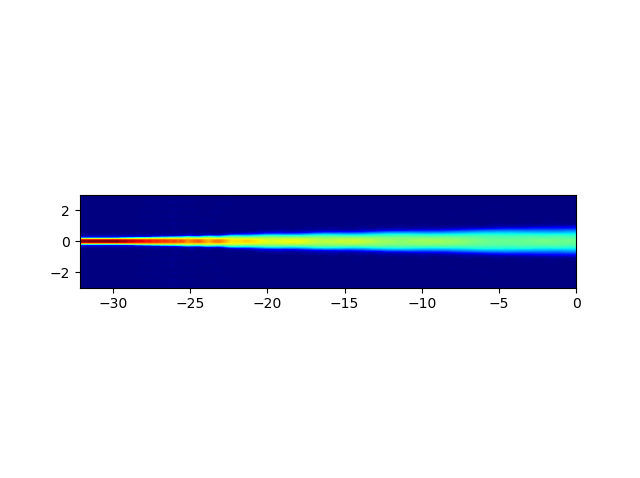
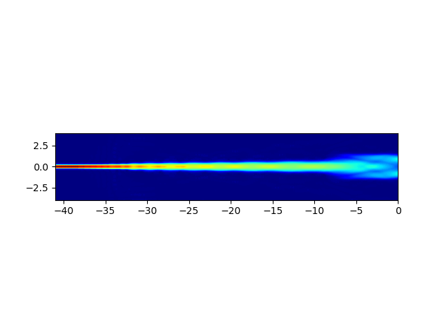
We can also check a top-down view of the field propagating through the whole aperture structure:
# Field propagated from input to the aperture
print("Simulating aperture field propagation...\n")
fields_2d = fieldmodel.get_aperture_fields2d(mode=0, environment=env)
fields_2d.visualize()
Note that this field profile is not necessarily exactly the same as the ground mode profile of the transition’s output! Instead, it is the field profile expanded into the slab modes, after having taken the overlap integral with those slab modes.
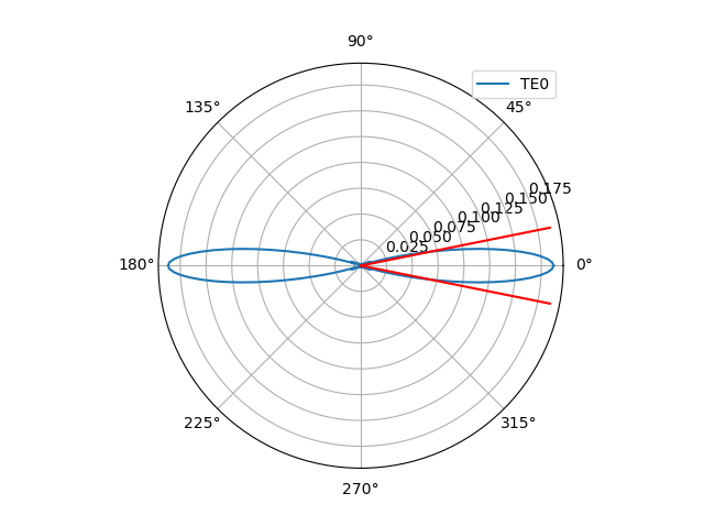
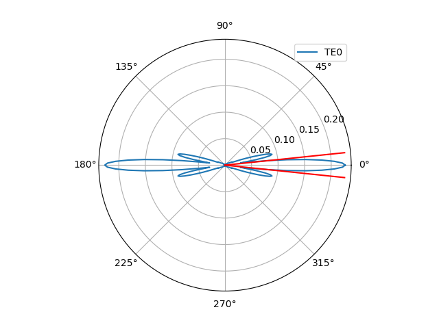
Finally, we can have a look at the far field of the aperture and its \(1/e^2\) divergence angle:
# Far field of the aperture
print("Simulating far field of the aperture...\n")
fields_ff = fieldmodel.get_far_field(mode=0, environment=env)
divergence_angle = fields_ff.divergence_angle(slab_mode="TE0", method="e_sq")
print(divergence_angle)
fields_ff.visualize()
If you are designing your own apertures, it is important that you carefully check the results of the simulation in order to make sure that the simulations are correct and that your aperture is performant. We recommend that you follow the tutorial on building your own aperture in that case.
The far field is also calculated and, in the following step, it is used to calculate the design parameters of the AWGs. In the final step, for simulating the AWG, the free propagation region is simulated by launching the field profile into the free propagation region. The S-matrix of the free propagation region is calculated using overlap integrals with field profile of the output aperture. Please see this tutorial on the simulation of AWGs for more information.
Test your knowledge
Run the following file:
luceda-academy/training/topical_training/cwdm_awg/components/plot_aperture.py
Change
taper_length. What is the influence on the transmission? Can the taper be made shorter?Change
aperture_core_widthWhat is the influence on the transmission?
Multimode interference aperture
A well-known technique to achieve a broad transmission band around each channel wavelength, is to use a multimode interference (MMI) aperture at the input side while keeping the regular aperture at the output side.
The channel spectral response is a convolution between the output’s field profile with the image of the input field on the output focal plane (multiplied by the array factor of the phased array). Hence, if we design the MMI such that the field launched into the input star coupler has two lobes with a lower field strength in the center, this convolution will yield a more flat-top behavior. This will come at the expense of somewhat higher insertion loss.
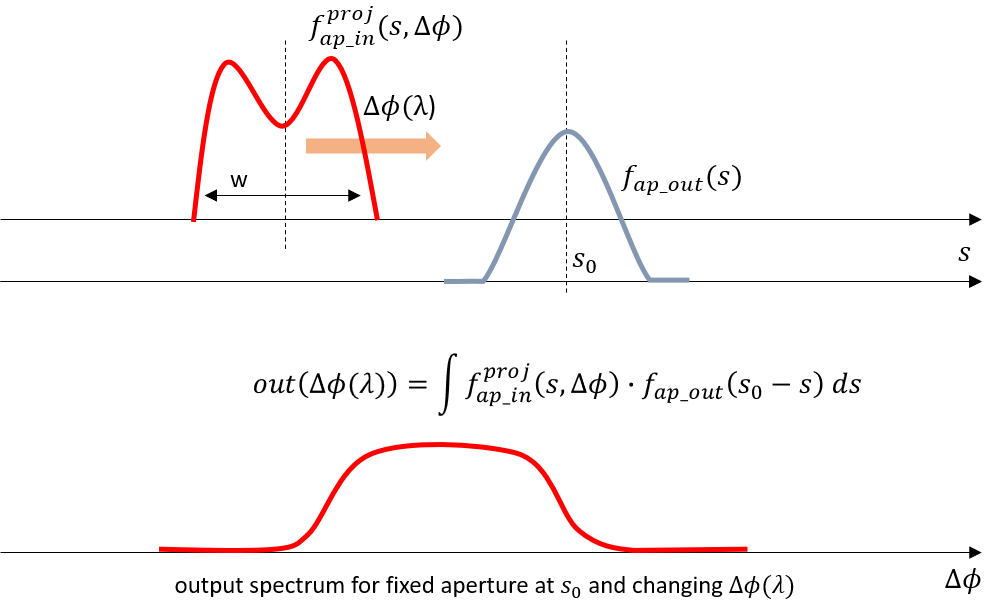
Flat-top behavior with an MMI input: the convolution of the projection of the input field (output of the MMI) with the output aperture’s field along the output curve yields a flat-top spectrum.
The physical explanation of this is as follows. As the wavelength is swept, the focal point of the light in the output star coupler is swept along the output plane of the output star coupler. This means that the field at the output of the star coupler will be swept across the field of the mode(s) of the aperture output. The transmission is provided by an overlap integral between the two fields. This means that, if you choose the parameters of the MMI aperture correctly, the overlap remains constant while the wavelength is swept in a certain region around the center wavelength. This leads to a flat-top transmission band at the channels.
The SiFab PDK contains a predefined si_fab_awg.all.SiRibMMIAperture.
Like for the regular aperture, we can instantiate it and visualize its layout top-down.
Then we can plot the output field profile, the 2D top-down view of the fields and the far-field.
import si_fab.all as pdk  # noqa: F401
from si_fab_awg.all import SiSlabTemplate, SiRibMMIAperture
import ipkiss3.all as i3
import numpy as np

wavelengths = np.linspace(1.25, 1.35, 100)
center_wavelength = 1.3

slab_tmpl = SiSlabTemplate()
slab_tmpl.SlabModesFromCamfr(wavelengths=wavelengths)

aperture = SiRibMMIAperture(slab_template=slab_tmpl, mmi_length=9.0, wire_width=0.4)

# Layout
print("Instantiating aperture layout...\n")
aperture_lay = aperture.Layout()
aperture_lay.visualize(annotate=True)
aperture_lay.visualize_2d(process_flow=i3.TECH.VFABRICATION.PROCESS_FLOW_FEOL)

# Field model
fieldmodel = aperture.FieldModelFromCamfr()
env = i3.Environment(wavelength=center_wavelength)

# Field profile at the aperture
print("Simulating field profile at aperture...\n")
fields = fieldmodel.get_fields(mode=0, environment=env)
fields.visualize()

# Field propagated from input to the aperture
print("Simulating aperture field propagation...\n")
fields_2d = fieldmodel.get_aperture_fields2d(mode=0, environment=env)
fields_2d.visualize()

# Far field of the aperture
print("Simulating far field of the aperture...\n")
fields_ff = fieldmodel.get_far_field(mode=0, environment=env)
divergence_angle = fields_ff.divergence_angle(slab_mode="TE0", method="e_sq")
print(divergence_angle)
fields_ff.visualize()
With this MMI aperture, the regular aperture and the slab template, we have now reviewed the components that are needed to design the star couplers of the AWG.
Test your knowledge
Run the following file:
luceda-academy/training/topical_training/cwdm_awg/components/plot_mmi_aperture.py
Change
mmi_length. What is the influence on the transmission?
Waveguides
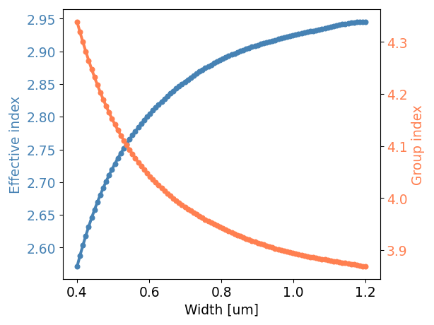
Finally, we need a model for the waveguides, so that the waveguide array can be correctly designed, generated and simulated. The waveguide’s wavelength-dependent effective index model will be used to design the length increments between successive waveguides to match the required specifications.
SiFab already comes with a strip waveguide template with an appropriate model. Here, we visualize its effective index and group index at 1.3 um wavelength:
import si_fab.all as pdk
import ipkiss3.all as i3
import numpy as np
import pylab as plt

center_env = i3.Environment(wavelength=1.3)
widths = np.linspace(0.4, 1.2, 100)
neffs = []
ngs = []

for w in widths:
    tmpl = pdk.SiWireWaveguideTemplate()
    tmpl.Layout(core_width=w)
    tmpl_cm = tmpl.CircuitModel()
    neffs.append(tmpl_cm.get_n_eff(center_env))
    ngs.append(tmpl_cm.get_n_g(center_env))

fig, ax1 = plt.subplots()

ax1.plot(widths, neffs, "o-", markersize=5, linewidth=3, color="steelblue")
ax1.set_xlabel("Width [um]", fontsize=14)
ax1.set_ylabel("Effective index", color="steelblue", fontsize=14)
ax1.tick_params(axis="y", labelcolor="steelblue", labelsize=14)
ax1.tick_params(axis="x", labelcolor="black", labelsize=14)

ax2 = ax1.twinx()
ax2.plot(widths, ngs, "o-", markersize=5, linewidth=3, color="coral")
ax2.set_ylabel("Group index", color="coral", fontsize=14)
ax2.tick_params(axis="y", labelcolor="coral", labelsize=14)

fig.tight_layout()
plt.show()
luceda-academy/training/topical_training/cwdm_awg/components/plot_wg_model.py
Test your knowledge
Run the following file:
luceda-academy/training/topical_training/cwdm_awg/components/plot_wg_model
Conclusion
Having defined and reviewed all the subcomponent models, we can now start the synthesis phase of the AWG.