Multimode interferometer
SiFab contains four multimode interferometers (MMI):
MMI1x2: a fully parametric MMI, with one input and two outputs.
MMI1x2Optimized1310: an 1x2 MMI with locked properties optimized for 1310 micrometers with CAMFR.
MMI1x2Optimized1550: an 1x2 MMI with locked properties optimized for 1550 micrometers with CAMFR.
MMI1x2Optimized1550FDTD: an 1x2 MMI with locked properties optimized for 1550 micrometers with FDTD.
The section Simulation and regeneration of the data files explains how to simulate and regenerate the simulation data of an MMI. The section Creating a new optimized MMI explains how to create a new optimized MMI with different layout parameters.
MMI1x2
This is an MMI with fully customisable layout.
This class has a circuit model where the following parameters can be provided to perform a circuit simulation of the MMI: center_wavelength, transmission, reflection_in and reflection_out.
Reference
Click on the name of the component below to see the complete PCell reference.
MMI with 1 input and 2 outputs. |
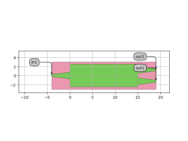
Example
from si_fab import all as pdk

mmi = pdk.MMI1x2(
    trace_template=pdk.SiWireWaveguideTemplate(),
    width=5.0,
    length=15.0,
    taper_width=1.5,
    taper_length=4.0,
    waveguide_spacing=2.5,
)
mmi_lv = mmi.Layout()
mmi_lv.visualize(annotate=True)
MMI Model
For the 1x2 MMI, we use the following model:
where \(t\) is the transmission (through), \(r_1\) is the reflection at the input and \(r_2\) is the reflection at the output. \(t\), \(r_1\), \(r_2\) are dispersive with respect to wavelength.
MMI1x2Optimized1550
This MMI inherits from MMI1x2.
All the properties are locked, because the layout has been optimized to obtain maximum transmission at 1550 nm wavelength.
The optimization and simulation of this component have been performed using CAMFR, the built-in 2D solver of IPKISS.
After the simulation, a fitting is performed of the transmission and reflections as a function of wavelength.
The fitting coefficients for \(t\), \(r1\), \(r2\) are stored and used by Caphe to calculate the S-matrix and perform a circuit simulation.
Reference
Click on the name of the component below to see the complete PCell reference.
MMI1x2 with layout parameters optimized for maximum transmission at 1550 nm. |
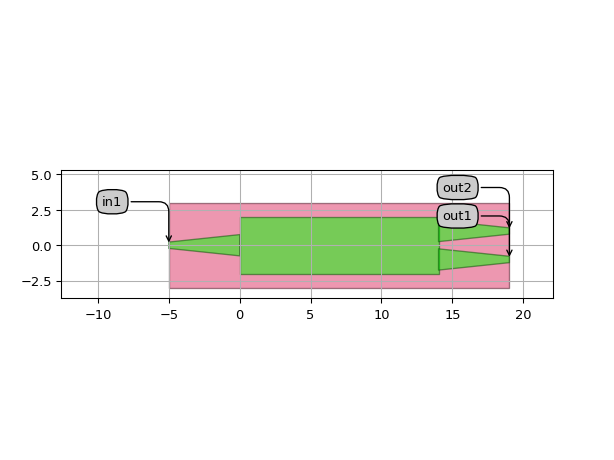
Example
from si_fab import all as pdk
import numpy as np
mmi = pdk.MMI1x2Optimized1550()
mmi_lv = mmi.Layout()
mmi_lv.visualize(annotate=True)
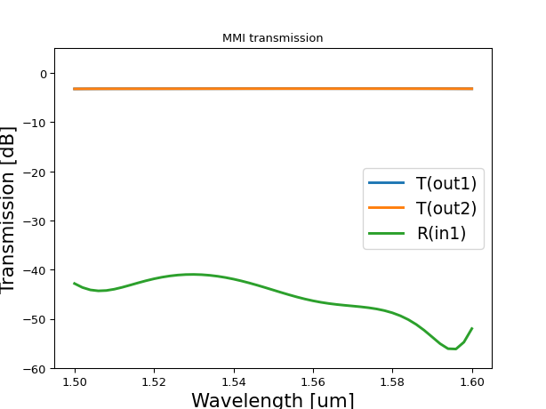
mmi_cm = mmi.CircuitModel()
wavelengths = np.linspace(1.5, 1.6, 51)
S = mmi_cm.get_smatrix(wavelengths=wavelengths)
S.visualize(
term_pairs=[
("in1", "out1"), # transmission 1
("in1", "out2"), # transmission 2
("in1", "in1"), # reflection
],
scale="dB",
title="MMI transmission",
yrange=(-60, 5),
)
MMI1x2Optimized1550FDTD
This MMI inherits from MMI1x2.
All the properties are locked, because the layout has been optimized to obtain maximum transmission at 1550 nm wavelength.
The optimization and simulation of this component have been performed using Luceda Link for Tidy3D, a third-party FDTD solver.
After the simulation, a BSplineSModel is built from the S-matrix obtained.
This model is available in the PCell’s CircuitModel, so that it can be used by Caphe to perform a circuit simulation.
Note
The simulation data included is hypothetical and for educational purposes only.
Note
While it is a common and good practice to include the wavelength for which the device has been optimized in its name (1550 in this case), it is rather uncommon to have components optimized using different solvers. In this case, two separate components have been created for demonstration and training purposes. For more details, see the following tutorials: CAMFR (EME) and FDTD.
Reference
Click on the name of the component below to see the complete PCell reference.
MMI1x2 with layout parameters optimized for maximum transmission at 1550 nm. |
Example
from si_fab import all as pdk
import numpy as np

mmi = pdk.MMI1x2Optimized1550FDTD()
mmi_lv = mmi.Layout()
mmi_lv.visualize(annotate=True)

mmi_cm = mmi.CircuitModel()

wavelengths = np.linspace(1.5, 1.6, 101)
S = mmi_cm.get_smatrix(wavelengths=wavelengths)
S.visualize(scale="dB", term_pairs=[("in1", "out1"), ("in1", "out2"), ("in1", "in1")])
MMI1x2Optimized1310
Same as MMI1x2Optimized1550 but optimized at 1310.
Reference
Click on the name of the component below to see the complete PCell reference.
MMI1x2 with layout parameters optimized for maximum transmission at 1310 nm. |
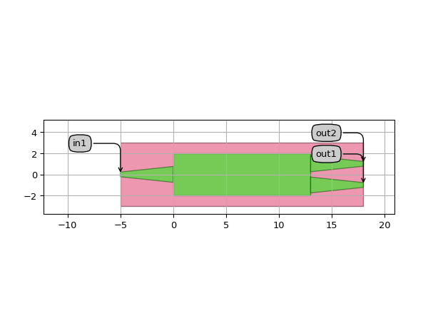
Example
from si_fab import all as pdk
import numpy as np

mmi = pdk.MMI1x2Optimized1310()
mmi_lv = mmi.Layout()
mmi_lv.visualize(annotate=True)

mmi_cm = mmi.CircuitModel()

wavelengths = np.linspace(1.26, 1.36, 1001)
S = mmi_cm.get_smatrix(wavelengths=wavelengths)
S.visualize(
    term_pairs=[
        ("in1", "out1"),  # transmission 1
        ("in1", "out2"),  # transmission 2
        ("in1", "in1"),  # reflection
    ],
    scale="dB",
    title="MMI transmission",
    yrange=(-70, 5),
)
Simulation and regeneration of the data files
CAMFR (EME) simulations
The simulation data of MMI1x2Optimized1550 and MMI1x2Optimized1310 are obtained with CAMFR and can be regenerated.
This can be done with the regenerate_mmi() function using the script regenerate_mmi_1x2_optimized_1550.py contained in si_fab/components/mmi/regeneration.
The user can specify the following options:
mmi_class: the mmi to regenerate. The name should not contain parentheses ().wavelengths: list of wavelengths at which the simulation should be run.center_wavelength: the center wavelength of the component.resimulate: boolean. If True, the MMI will be simulated at all thewavelengths. A fitting of the transmission as a function of wavelength is performed and the results are stored in a file in data/component_name.z.plot: boolean. If True, it plots the results of the simulation.
For a complete tutorial on how to design and optimize the 1x2 MMI, check out MMI: Device Simulation for Layout Optimization.
Reference
Click on the name of the functions below to see the complete API reference of the simulation and regeneration recipes.
|
It simulates a symmetric splitter and returns the transmission and reflection. |
|
It regenerates the simulation fitting data and/or the plots of the optimized MMI. |
FDTD simulations
The simulation data of MMI1x2Optimized1550FDTD are obtained with Tidy3D and can be regenerated.
The optimization script optimize_mmi_1x2_1550_tidy3d.py is contained in si_fab/components/mmi/optimization.
See below the API reference of the simulation recipe.
Reference
|
Performs an FDTD simulation of a given MMI layout. |
Creating a new optimized MMI
The user has the possibility of exploring the MMI and creating a new optimized component with different optimized parameters.
The optimization can be performed by running the script optimize_mmi_1x2_1550.py contained in si_fab/components/mmi/optimization.
Some layout parameters are kept fixed (taper_width, taper_length, width), while the length of the MMI (length) and the spacing between the output waveguides (wg_spacing) are optimized to obtain maximum transmission.
The new layout parameters can be used to create an optimized MMI with new default values.
The simulation data of this new component can be generated by running the regeneration script and should be used to perform circuit simulations of this new component.
For a complete tutorial on how to design and optimize the 1x2 MMI, check out MMI: Device Simulation for Layout Optimization.
Reference
Click on the name of the function below to see the complete API reference of the optimization recipe.
Note
The above simulation results are artificial results as they’re based on fictional technology and components. These only serve demonstration purposes.