6. AWG demultiplexer with AMF PDK
Note
This application example requires the Luceda PDK for AMF. Please click here to obtain the PDK.
In this tutorial, we provide an example of how to implement arrayed waveguide gratings (AWGs) for wavelength division multiplexing on the Luceda PDK for AMF.
6.1. Designing the AWG
The AWGs targets the IEEE 400Gb Ethernet standard 400GBase-LR8 specifications just as for the Arrayed waveguide grating (AWG) demultiplexer tutorial and so targets the same channel wavelengths. We are going to design two AWGs, one with an FSR of 10400 GHz and the other with an FSR of 12000 GHz. Please note that this does not represent a finished off-the-shelf design, you will need to tweak and simulate it for your purposes and validate it in hardware. To design the AWGs we use the following subcomponents from the Luceda PDK for AMF:
RIB_WG_TEMPLATE_410: This is the trace template we use for our waveguide. It has a width of 4.1 um and is intended for O-band specifications.SiSlabTemplate: This is our slab template.SiSlabWaveguideAperture: This is the aperture class.
We set the circuit model of our RIB_WG_TEMPLATE_410 by providing it with the (approximate) effective and group indices of 2.6 and 4.3 at a center wavelength of 1.3 um.
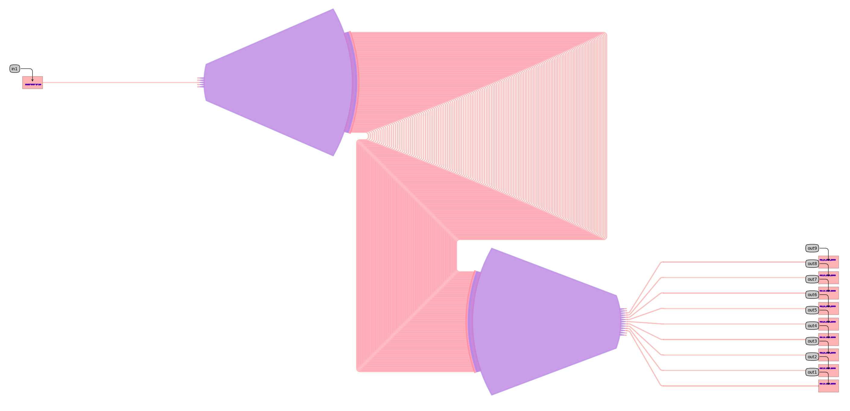
In the finalization step, we route the AWG to the grating couplers of the class AMF_Si_GC1D_Oband in the AMF PDK.
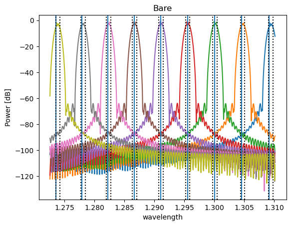
We show below the layout of one of the final routed AWGs together with the simulation results:
When we implement this in the code, everything else is the same as in the Arrayed waveguide grating (AWG) demultiplexer tutorial, with some slight changes in implementation. We show the full script below:
import amfsip.all as pdk  # noqa: F401
from ipkiss3 import all as i3
import numpy as np
import os
from generate import generate_awg
from simulate import simulate_awg
from finalize import finalize_awg
from analyze import analyze_awg

# Actions
generate = True
simulate = True
analyze = True
finalize = True
plot = True

# Specifications
fsrs = [10400, 12000]

for fsr in fsrs:
    design_name = "awg_{}".format(fsr)
    print("Designing {}...".format(design_name))
    # Creating a folder for results
    this_dir = os.path.abspath(os.path.dirname(__file__))
    designs_dir = os.path.join(this_dir, "gds_to_merge")
    if not os.path.exists(designs_dir):
        os.mkdir(designs_dir)
    save_dir = os.path.join(designs_dir, design_name)
    if not os.path.exists(save_dir):
        os.mkdir(save_dir)

    # Simulation specs
    wavelengths = np.linspace(1.26, 1.32, 1000)

    # Bare AWG
    if generate:
        awg = generate_awg(fsr=fsr, plot=plot, save_dir=save_dir, tag="bare")
    if simulate:
        smat = simulate_awg(awg=awg, wavelengths=wavelengths, save_dir=save_dir, tag="bare")
    else:
        path = os.path.join(save_dir, "smatrix_bare.s10p")
        smat = i3.device_sim.SMatrix1DSweep.from_touchstone(path, unit="um") if os.path.exists(path) else None

    if analyze:
        analyze_awg(smat, peak_threshold=-10.0, plot=plot, save_dir=save_dir, tag="bare")

    # Finished AWG
    if finalize:
        if generate:
            finalized_awg = finalize_awg(awg=awg, name=design_name, plot=plot, save_dir=save_dir, tag="finalized")

            print("Extract size info {}".format(design_name))

            layout = finalized_awg.get_default_view(i3.LayoutView)

            # Extract file info and export it
            si = layout.size_info()
            size_info_file = os.path.join(save_dir, "awg_{}_finalized_si.txt".format(fsr))
            np.savetxt(size_info_file, si.bounding_box.points)

        if simulate:
            smat_finalized = simulate_awg(
                awg=finalized_awg,
                wavelengths=wavelengths,
                save_dir=save_dir,
                tag="finalized",
            )
        else:
            path = os.path.join(save_dir, "smatrix_finalized.s10p")
            smat_finalized = (
                i3.device_sim.SMatrix1DSweep.from_touchstone(path, unit="um") if os.path.exists(path) else None
            )

        if analyze:
            analyze_awg(smat_finalized, peak_threshold=-20.0, plot=plot, save_dir=save_dir, tag="finalized")

    print("Done")
6.2. Preparing to tape-out
In order to prepare for the tape-out, we want to place the layout of both the AWGs that we generate onto a design frame.
For this, we use the AMF_MPW1_Half_Frame PCell from the AMF PDK.
We use the regenerate.py scripts to create the GDS files and then merge them together using the execute_merge.py script:
from amfsip import all as pdk  # noqa: F401
from ipkiss3 import all as i3
import os
import numpy
from gds_utils.klayout.merge import merge_with_klayout

base_dir = os.path.dirname(os.path.abspath(__file__))
designs = []

# Add the frame
size_info_frame = i3.size_info_from_numpyarray(
    numpy.loadtxt(open(os.path.join(base_dir, "frame", "gds_to_merge", "frame_si.txt")))
)
designs.append(
    {
        "source_path": os.path.join(base_dir, "frame", "gds_to_merge", "frame.gds"),
        "prefix": "TEMPLATE",
        "transformations": [[0.0, 0.0, 0.0, False]],
    }
)

folder_path = "awg_amf_fsr_sweep/gds_to_merge"

# Design 1
design_name = "awg_10400"
gds_file = "{}_finalized.gds".format(design_name)
design_path = os.path.join(folder_path, design_name)
size_info_awg1 = i3.size_info_from_numpyarray(
    numpy.loadtxt(open(os.path.join(design_path, "{}_finalized_si.txt".format(design_name))))
)
spacing = 200  # Desired spacing between designs
margin_x = 700  # Margin to the block edge
margin_y = 400
print(os.path.join(design_path, gds_file))
print(design_name.upper())

designs.append(
    {
        "source_path": os.path.join(design_path, gds_file),
        "prefix": design_name.upper(),
        "transformations": [[0.0 + margin_x, 0.0 - size_info_awg1.south + margin_y, 0.0, False]],
    }
)


# Design 2
design_name = "awg_12000"
gds_file = "{}_finalized.gds".format(design_name)
design_path = os.path.join(folder_path, design_name)
size_info_awg2 = i3.size_info_from_numpyarray(
    numpy.loadtxt(open(os.path.join(design_path, "{}_finalized_si.txt".format(design_name))))
)
print(os.path.join(design_path, gds_file))
print(design_name.upper())
designs.append(
    {
        "source_path": os.path.join(design_path, gds_file),
        "prefix": design_name.upper(),
        "transformations": [
            [
                0.0 + margin_x,
                0.0 + margin_y + spacing - size_info_awg1.south + size_info_awg2.north - size_info_awg2.south,
                0.0,
                False,
            ]
        ],
    }
)

merge_with_klayout(
    designs=designs,
    keep_temp_files=False,
    top_cell_name="AMF_CWDM_AWG",
    grid_per_unit=int(round(i3.get_grids_per_unit())),
    unprefixed_cells=["AMF_Si_GC1D_Oband_v3p0"],
    output_layer_map=i3.TECH.GDSII.EXPORT_LAYER_MAP,
    output_gds="tapeout_amf_cwdm_merged.gds",
)
For more details about the mask merging procedure, please follow the tutorial Several contributions to one tape-out run.