4. MMI simulation and optimization
In the previous section, you have learned how to add a circuit model to a component and run a frequency-domain simulation. The MMI we designed and simulated has all the right ingredients, i.e. Layout View, Netlist View and Circuit Model View using a custom Compact Model, but it is not yet optimized.
In this session we are going to see how to simulate the MMI using CAMFR. Afterwards, we will use this simulation recipe to optimize the layout parameters of the MMI to maximize the transmission.
4.1. Simulation with CAMFR
CAMFR is the built-in 1D mode solver and 2D EME propagation simulation tool of IPKISS. It is based on frequency-domain eigenmode expansion techniques and it can calculate:
the scattering matrix of a structure;
the field inside a structure, for any given excitation;
band diagrams of an infinite periodic structure;
threshold material gain and resonance wavelength of laser modes;
the response to a current source in an arbitrary cavity;
structures containing a semi-infinite repetition of a basic period.
For more information about CAMFR, clik here.
The simulation recipe of the MMI is defined directly inside the PDK, which is SiFab in our case. As mentioned at the beginning of this tutorial, we neatly organize the simulation recipe in a dedicated simulation sub-folder:
mmi
├── data
├── doc
├── optimization
├── pcell
├── regeneration
├── simulation
│   ├── __init__.py
│   └── simulate_camfr.py
└── __init__.py
This way, if you share the PDK with other people, everyone will be able to run simulations without having to define everything from scratch.
The file simulate_camfr.py contains a function which defines the MMI simulation recipe.
This function is called simulate_splitter_by_camfr and accepts the following parameters as input:
layout: the Layout View of the component you wish to simulate (the MMI in this case);wavelengths: a set of wavelengths to use for the simulation;num_mod: number of modes to simulate (default is 10);discretization_res: discretization resolution of the structure (default is 20);north: north-bound limit of the structure (default is 4.0), which is used to define the simulation window;plot: if True, it plots the fields (default is True).
def simulate_splitter_by_camfr(
    layout,
    wavelengths,
    num_modes=10,
    discretization_res=20,
    north=4.0,
    plot=True,
):
Because in this case the MMI is symmetric to the x-axis, the simulation recipe is defined to simulate only the top half of the structure. This allows to save simulation time and resources. The simulation returns a list of values of the transmission between the input and the output port and the reflection at the input port at each specified wavelength:
        trans_list.append(abs(camfr_stack.T12(0, 0)) / (2.0**0.5))
        refl_list.append(abs(camfr_stack.R12(0, 0)))

    return trans_list, refl_list
This simulation recipe can now be imported in a separate file to run the simulation:
First, we instantiate the MMI and the Layout View.
training/topical_training/device_optimization_mmi/explore_mmi_camfr_simulation.pymmi = pdk.MMI1x2( trace_template=pdk.SiWireWaveguideTemplate(), width=5.0, length=15.0, taper_width=1.5, taper_length=4.0, waveguide_spacing=2.5, ) mmi_lv = mmi.Layout()
We define the simulation wavelengths and the center wavelength. Then, we run the simulation in the selected wavelength range on the layout defined in
mmi_lv. Note that the north-bound limit of the simulation is extracted directly from the layout of the MMI, to avoid mistakes.wavelengths = np.arange(1.5, 1.6, 0.01) center_wavelength = 1.55 print("Simulating...") sim_result = simulate_splitter_by_camfr( layout=mmi_lv, wavelengths=wavelengths, num_modes=20, north=0.5 * mmi_lv.size_info().get_height(), plot=False, ) print("Done")
We perform a polynomial fitting of the simulated values of transmission versus wavelength, and of the simulated values of reflection (at the input port) versus wavelength.
pol_trans = np.polyfit(wavelengths - center_wavelength, sim_result[0], 7)
pol_refl_in = np.polyfit(wavelengths - center_wavelength, sim_result[1], 7)
# The value of pol_refl_out is not extracted from the CAMFR simulation but we assume it's the same as pol_refl_in
pol_refl_out = pol_refl_in
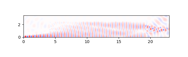
We run the CAMFR simulation at 1550 nm to visualize the field propagation.
simulate_splitter_by_camfr(
    layout=mmi_lv,
    wavelengths=np.array([center_wavelength]),
    num_modes=20,
    north=0.5 * mmi_lv.size_info().get_height(),
    plot=True,
)
We instantiate the Circuit Model of the MMI using the polynomial coefficients calculated from the simulation results.
mmi_cm = mmi.CircuitModel(
    center_wavelength=center_wavelength,
    transmission=pol_trans,
    reflection_in=pol_refl_in,
    reflection_out=pol_refl_out,
)
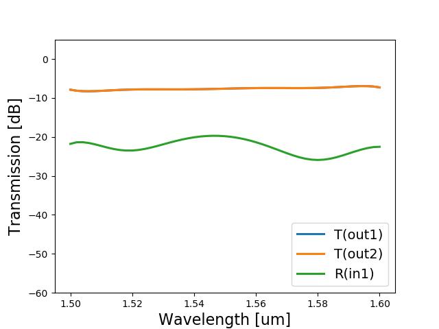
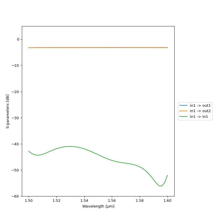
We extract the S-matrix of the MMI and plot the transmission between the input and the output ports, and the reflection at the input port.
wavelengths = np.linspace(1.5, 1.6, 51)
S = mmi_cm.get_smatrix(wavelengths=wavelengths)
S.visualize(
    term_pairs=[
        ("in1", "out1"),  # transmission 1
        ("in1", "out2"),  # transmission 2
        ("in1", "in1"),  # reflection
    ],
    scale="dB",
    yrange=(-60, 5),
)
Now we have a circuit simulation that corresponds to the layout of the instantiated MMI PCell. However, the geometry of the MMI is not optimized. This is visible both in the plot of the field propagation and in the low transmission between the input and the output ports. Therefore, the next step is the optimization of the MMI.
4.2. Optimization
To optimize the MMI, we define an optimization function that is included in the MMI folder of the PDK.
mmi
├── data
├── doc
├── optimization
│   ├── __init__.py
│   ├── opt_utils.py
│   └── optimize_mmi_1x2.py
├── pcell
├── regeneration
├── simulation
└── __init__.py
The purpose of the optimization is to maximize the transmission of the MMI by varying the MMI length and the spacing between the output waveguides,
while keeping the wavelength, the trace template, the MMI width, the taper width and the taper length fixed.
Different input parameters can be specified, such as initial values for the MMI width and the waveguide spacing, the max number of iterations, verbose (True or False) and plot (True or False).
The optimization is performed through scipy.optimize.minimize() using the Nelder-Mead algorithm (see doc).
The optimization function returns the optimized values of MMI length and output waveguide spacing.
The optimization function can be found in: pdks/si_fab/ipkiss/si_fab/components/mmi/optimization/opt_utils.py.
Let’s see how to use it.
First, we assign values to the parameters that are not being optimized.
Then, we call the optimize_mmi function and store the results in the res variable.
To finish, we can add print statements to visualize a comprehensive list of the layout parameters needed
to design the optimized MMI.
tt = pdk.SiWireWaveguideTemplate()
wavelength = 1.55
taper_length = 5.0
width = 4.0

res = optimize_mmi(
    mmi_class=pdk.MMI1x2,
    width=width,
    taper_length=taper_length,
    trace_template=tt,
    wavelength=wavelength,
    initial_wg_spacing=2.0,
    initial_length=10.0,
    initial_taper_width=1.5,
    verbose=True,
)

print("OPTIMIZATION RESULTS")
print(f"Optimal length = {res[0]} um")
print(f"Optimal waveguide_spacing = {res[1]} um")
print(f"Optimal taper width = {res[2]} um")
print(f"width = {width} um")
print(f"taper_length = {taper_length} um")
In this case, the optimized length is 14.02 um, the optimized waveguide spacing is 2.007 um and the optimized taper width is 1.499.
4.3. PCell of the optimized MMI
Now that the layout parameters of the MMI are optimized, we can define a component in SiFab with fixed properties. This approach is often used when developing component libraries to ensure that the fabricated component behaves as expected and the layout parameters are not changed erroneously.
To do this, the concept of hierarchy in IPKISS is used (see Layout - Advanced).
We define a PCell called MMI1x2Optimized1550 which inherits from MMI1x2 and therefore can use the same Layout View, Netlist View and Circuit Model View defined for MMI1x2.
We assign fixed values to all the properties and we lock them using @i3.lock_properties() so they can’t be modified.
In the Circuit Model View we load the transmission and the reflection coefficients from a data file created after simulating the component.
Let’s see how this is done.
@i3.lock_properties()
class MMI1x2Optimized1550(MMI1x2):
    """MMI1x2 with layout parameters optimized for maximum transmission at 1550 nm.
    transmission and reflection_in (reflection at input port) are extracted from data from a CAMFR simulation;
    reflection_out (reflection at output port) is not simulated therefore a dummy number is passed.
    """

    data_tag = i3.LockedProperty()

    def _default_data_tag(self):
        return "mmi_1x2_optimized_1550"

    def _default_name(self):
        return self.data_tag.upper()

    def _default_trace_template(self):
        tt = SiWireWaveguideTemplate(name=self.name + "_tmpl")
        tt.Layout(core_width=0.45)
        return tt

    def _default_width(self):
        return 4.0

    def _default_length(self):
        return i3.snap_value(14.0258356928 / 2.0) * 2.0  # Snap to twice the grid size so that the edges are on the grid

    def _default_taper_width(self):
        return i3.snap_value(1.49982527224 / 2.0) * 2.0  # Snap to twice the grid size so that the edges are on the grid

    def _default_taper_length(self):
        return 5.0

    def _default_waveguide_spacing(self):
        return i3.snap_value(2.00712657136 / 2.0) * 2.0  # Snap to twice the grid size so that the edges are on the grid

    class CircuitModel(MMI1x2.CircuitModel):
        @i3.cache()
        def _get_data(self):
            return get_data(data_tag=self.data_tag)

        def _default_center_wavelength(self):
            c_wl, _, _ = self._get_data()
            return c_wl

        def _default_transmission(self):
            _, trans, _ = self._get_data()
            return trans

        def _default_reflection_in(self):
            _, _, refl_in = self._get_data()
            return refl_in

        def _default_reflection_out(self):
            return np.array([0.0])
All we have left to do is to make sure that the correct data is stored in the right file and in the right folder so that the function get_data() can find it and we can instantiate and simulate this component correctly.
To achieve this, a regeneration script is used, which is also included in the MMI folder in the SiFab PDK:
mmi
├── data
│   └── mmi_1x2_optimized.z
├── doc
├── optimization
├── pcell
├── regeneration
│   ├── __init__.py
│   ├── regen_utils.py
│   └── regenerate_mmi_1x2.py
├── simulation
└── __init__.py
First, a regenerate_mmi function is defined in the file regen_utils.py.
The goal of this function is to regenerate the simulation fitting data and/or the plots of the optimized MMI MMI1x2Optimized1550 that is passed to the function as a parameter.
This function is then imported in regenerate_mmi_1x2.py
By running this script, you are sure that the data used to simulate the MMI1x2Optimized1550 component is always up-to-date.
The data is stored in si_fab/components/mmi/data, as can be seen from the folder structure above.
After regenerating the simulation data, we can create a new script to explore the layout and the simulation of the optimized MMI, as done earlier for the non-optimized MMI.
from si_fab import all as pdk
from si_fab.components.mmi.simulation.simulate_camfr import simulate_splitter_by_camfr
import matplotlib.pyplot as plt
import numpy as np
# 1. Layout
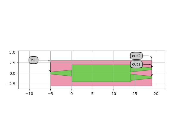
mmi = pdk.MMI1x2Optimized1550()
mmi_lv = mmi.Layout()
mmi_lv.visualize(annotate=True, show=True)
# 2. Circuit
mmi_cm = mmi.CircuitModel()
plt.figure()
# 3. Visualize the simulation at 1550 nm wavelength
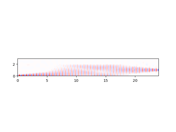
center_wavelength = mmi_cm.center_wavelength
simulate_splitter_by_camfr(
layout=mmi_lv,
wavelengths=np.array([center_wavelength]),
num_modes=20,
north=0.5 * mmi_lv.size_info().get_height(),
plot=True,
)
# 4. Plotting
wavelengths = np.linspace(1.5, 1.6, 51)
S = mmi_cm.get_smatrix(wavelengths=wavelengths)
S.visualize(
term_pairs=[
("in1", "out1"), # transmission 1
("in1", "out2"), # transmission 2
("in1", "in1"), # reflection
],
scale="dB",
yrange=(-60, 5),
)
Awesome! The reflection has been reduced by almost 20 dB and the transmission has improved by more than 5 dB.
The folder structure used in the SiFab PDK to illustrate the design, simulation and optimization of this 1x2 MMI can be re-used for any type of component. The simulation with CAMFR can also be replaced by a simulation with Ansys Lumerical or with CST Studio Suite ® by using the Luceda Links to these tools. For more info, check out our documentation (Lumerical and CST).