2. PCell: Layout
The first step towards designing the 1x2 MMI is to define the MMI PCell.
As mentioned in the previous section, every information concerning the PCell is added to the pcell subfolder:
mmi
├── data
├── doc
├── optimization
├── pcell
│   ├── __init__.py
│   ├── cell.py
│   └── cell_utils.py
├── regeneration
├── simulation
└── __init__.py
2.1. Define the PCell
We define a Python class derived from i3.PCell and we call it MMI1x2.
This is done inside the file cell.py.
Inside the MMI1x2 class we define a sub-class, class Layout, derived from i3.LayoutView.
This class will contain all the geometric information of the MMI.
class MMI1x2(i3.PCell):
    """MMI with 1 input and 2 outputs."""

    _name_prefix = "MMI1x2"
    trace_template = i3.TraceTemplateProperty(doc="Trace template of the access waveguide")
    width = i3.PositiveNumberProperty(default=4.0, doc="Width of the MMI section.")
    length = i3.PositiveNumberProperty(default=20.0, doc="Length of the MMI section.")
    taper_width = i3.PositiveNumberProperty(default=1.0, doc="Width of the taper.")
    taper_length = i3.PositiveNumberProperty(default=1.0, doc="Length of the taper")
    waveguide_spacing = i3.PositiveNumberProperty(default=2.0, doc="Spacing between the waveguides.")
    cladding_width = i3.PositiveNumberProperty(default=6.0, doc="Width of the cladding (device width).")

    def _default_trace_template(self):
        return SiWireWaveguideTemplate()

    def validate_properties(self):
        if self.width < self.waveguide_spacing + self.taper_width:
            raise i3.PropertyValidationError(
                self,
                "The sum of waveguide_spacing and taper_width exceeds the width of the MMI",
                {"width": self.width, "waveguide_spacing": self.waveguide_spacing, "taper_width": self.taper_width},
            )
        if self.waveguide_spacing < self.taper_width:
            raise i3.PropertyValidationError(
                self,
                "The waveguides will overlap: waveguide_spacing is too small or width is too big",
                {"taper_width": self.taper_width, "waveguide_spacing": self.waveguide_spacing},
            )
        return True

    class Layout(i3.LayoutView):
        def generate(self, layout):
            length = self.length
            width = self.width
            trace_template = self.trace_template
            cladding_width = self.cladding_width
            taper_length = self.taper_length
            taper_width = self.taper_width
            half_waveguide_spacing = 0.5 * self.waveguide_spacing
            core_layer = trace_template.core_layer
            cladding_layer = trace_template.cladding_layer
            core_width = trace_template.core_width

            # Si core
            layout += i3.Rectangle(
                layer=core_layer,
                center=(0.5 * length, 0.0),
                box_size=(length, width),
            )
            layout += i3.Wedge(
                layer=core_layer,
                begin_coord=(-taper_length, 0.0),
                end_coord=(0.0, 0.0),
                begin_width=core_width,
                end_width=taper_width,
            )
            layout += i3.Wedge(
                layer=core_layer,
                begin_coord=(length, half_waveguide_spacing),
                end_coord=(length + taper_length, half_waveguide_spacing),
                begin_width=taper_width,
                end_width=core_width,
            )
            layout += i3.Wedge(
                layer=core_layer,
                begin_coord=(length, -half_waveguide_spacing),
                end_coord=(length + taper_length, -half_waveguide_spacing),
                begin_width=taper_width,
                end_width=core_width,
            )
            # Cladding
            layout += i3.Rectangle(
                layer=cladding_layer,
                center=(0.5 * length, 0.0),
                box_size=(length + 2 * taper_length, cladding_width),
            )
            # Ports
            layout += i3.OpticalPort(
                name="in1",
                position=(-taper_length, 0.0),
                angle=180.0,
                trace_template=trace_template,
            )
            layout += i3.OpticalPort(
                name="out1",
                position=(length + taper_length, -half_waveguide_spacing),
                angle=0.0,
                trace_template=trace_template,
            )
            layout += i3.OpticalPort(
                name="out2",
                position=(length + taper_length, half_waveguide_spacing),
                angle=0.0,
                trace_template=trace_template,
            )
            return layout
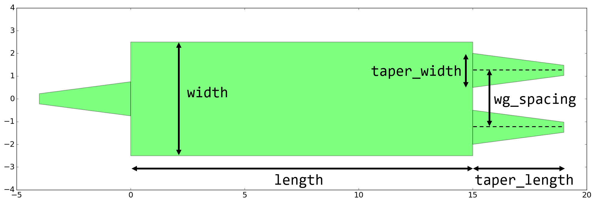
Let’s analyze the code above:
Properties. We define a list of properties that will be used to design the MMI. Five properties are defined using
i3.PositiveNumberPropertyand one is defined usingi3.TraceTemplateProperty. The order of these properties can be altered. Each property has a default value: if the user does not supply a value, this default will be used.Properties validation. We defined a
validate_propertiesmethod. This method is used to check that the layout is self-consistent. It will raise an error when the layout parameters of the MMI would cause a mistake in the design (e.g. when the sum of the waveguide spacing and the taper width exceeds the MMI width, or when the waveguide spacing is smaller than the taper width). This way, we can ensure that we don’t make mistakes when we instantiate the layout and assign values to the MMI properties.Layout class. We defined the Layout class inside the
MMI1x2PCell. This class is a Layout View. Here we use thegenerate(self, layout)method to define all the elements of our design.First, we added five geometric elements:
1 Rectangle, drawn on the core layer of our trace template (
core_layer), representing the multi-mode section of the MMI;3 Wedges, drawn on the core layer of our trace template (
core_layer), representing the tapers at the input and output;1 Rectangle, drawn on the cladding layer of our trace template (
cladding_layer), representing the cladding.
These five geometric elements are drawn using the properties defined at the beginning of the class
MMI1x2. For example, the length property is used by addressing it asself.length. Calculations of the dimension and position of the elements are performed with standard Python functions.After the geometric elements, we defined ports. Each port is created using
i3.OpticalPortand needs the following properties to be set:name: name of the port.position: position of the port.angle: direction in which a waveguide leaving the port has to go. 0 degrees is parallel to the x-axis, going eastwards.trace_template: it denotes the trace template of waveguide used at the port.
The trace template used is set at the PCell level and is passed on as a property.
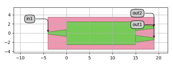
2.2. Visualize the layout
To visualize the layout, we first instantiate an object using the MMI1x2 PCell and then we instantiate the Layout class of this object.
When the MMI object is instantiated, the value of its properties can be modified, as shown below.
mmi = pdk.MMI1x2(
    trace_template=pdk.SiWireWaveguideTemplate(),
    width=5.0,
    length=15.0,
    taper_width=1.5,
    taper_length=4.0,
    waveguide_spacing=2.5,
)
mmi_layout = mmi.Layout()
We can now visualize the layout and export it to GDSII:
mmi_layout.visualize(annotate=True)
mmi_layout.write_gdsii("first_mmi.gds")
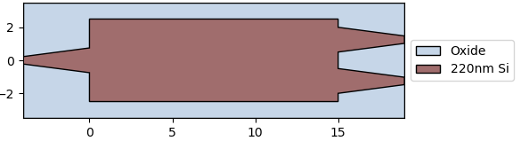
2.3. Virtual fabrication and cross section
In IPKISS, in addition to the visualize function, there is also the option to run a virtual fabrication using the visualize_2d function.
The output will show the actual fabricated layer stacks.
In our case, we can see that the MMI is fabricated on 220 nm Si and is surrounded by an oxide cladding.
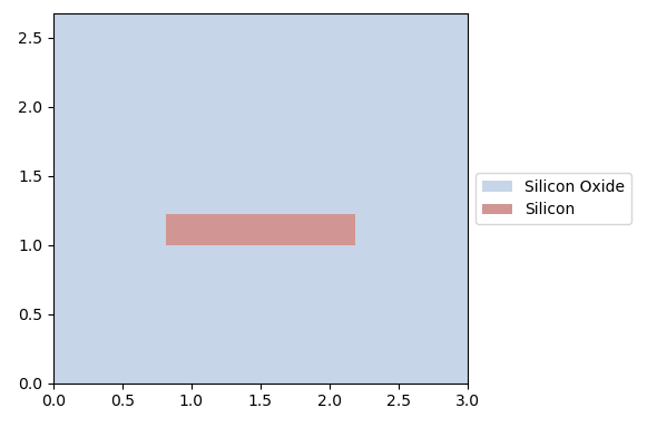
We can also visualize the cross section at specific coordinates.
mmi_layout.visualize_2d(process_flow=pdk.TECH.VFABRICATION.PROCESS_FLOW_FEOL)
mmi_layout.cross_section(