Grating Coupler Simulation
Note
This tutorial requires an installation of the Luceda Link for Tidy3D. Please contact us for a trial license.
This tutorial demonstrates how to perform a physical simulation of a grating coupler using Luceda Link for a third-party device simulation tool. The layout, simulation setup, and parameter sweep recipes are defined in IPKISS and then run in an external tool, in this case, Tidy3D. The simulation results can be retrieved and saved in IPKISS for further processing, such as plotting or building component models using the data. If you’re new to using Luceda Link for Tidy3D, we recommend starting with the Physical Device Simulation Flow tutorial, in particular the section on Tidy3D before proceeding.
We will cover three topics in this tutorial:
Exporting the layout and defining the near-field simulation settings.
Running a parameter sweep to optimize the grating coupler for maximum upward coupling.
Setting up a far-field simulation for the optimized grating coupler.
Exporting the layout and simulation settings
To begin, we define a general grating coupler PCell in IPKISS whose parameters can be adjusted. Once the layout is instantiated, we configure the simulation by placing a mode source at the in-plane port and a field monitor above the grating coupler. This setup is illustrated in the following image:
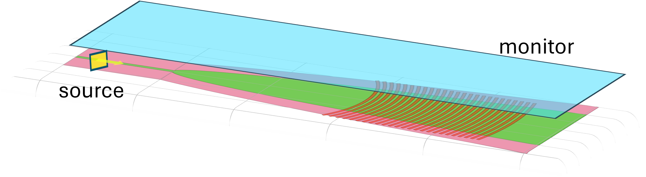
Figure 1. Simulation setup of the grating coupler, consisting of a grating coupler PCell, a mode source, and a field monitor.
This setup allows us to analyze the coupling efficiency and field distribution of the grating coupler.
IPKISS provides the capability to define macros, which allow a user to customize their simulation in the third-party solver. It usually consists of commands recognized by the solver, which can be used to automatically add new simulation components and configure different solver-specific options. Below are two macros used in this setup:
1. Mode Source Macro: This macro excites a desired mode at a specific position along a waveguide.
def mode_source(alignment_port: str, h_dev: float, wg_w: float, neff: float, x_port: float):
    """Macro to create a mode source to excite modal profile on finite extent transverse plane of a waveguide.

    Parameters
    ----------
    alignment_port : str
        Name of the port used to place the mode source (use center z position).
    h_dev : float
        Thickness of the layer where the device is placed to adjust the height of the source.
    wg_w : float
        Core width of the waveguide to adjust the height of the source.
    neff : float
        Target effective index of the mode generated by the mode source.
    x_port : float
        Position of the in-plane port of the grating coupler.

    Returns
    -------
        macro : i3.device_sim.Macro
    """
    commands = f"""
mode_spec = td.ModeSpec(num_modes=1, target_neff={neff})
source = td.ModeSource(
    center=({x_port} + 5, 0, ports_z_coord["{alignment_port}"]),
    size=(0, 4 * {wg_w}, 5 * {h_dev}),
    source_time=td.GaussianPulse(freq0=center_frequency, fwidth=0.5*center_frequency),
    direction="-",
    mode_spec=mode_spec,
    mode_index=0,
)

sources = [source]
"""

    macro = Macro(commands=commands.splitlines())
    return macro
2. Monitor Macro: This macro defines field and flux monitors to measure electromagnetic fields and power flux at a given height.
def monitors(h_dev: float, height: float, flux: bool = True, field: bool = True):
    """Macro to create an FDTD frequency-domain z-normal field monitor, flux monitor, or both,
    covering the full simulation window at a specified height.

    Parameters
    ----------
    h_dev : float
        Thickness of the layer where the device is placed.
    height : float
        Height of the monitors from top of the device.
    flux : boolean
        Set a flux monitor, default is True.
    flux : boolean
        Set a flux monitor, default is True.

    Returns
    -------
        macro : i3.device_sim.Macro
    """
    commands = []
    if flux:
        commands.extend(
            f"""
flux_monitor_xy = td.FluxMonitor(
    center=(0, 0, 1 + {h_dev} + {height}),
    size=(td.inf, td.inf, 0),
    freqs=[center_frequency],
    name="flux",
)
monitors = [flux_monitor_xy]
""".splitlines()
        )
    if field:
        commands.extend(
            f"""
field_monitor_xy = td.FieldMonitor(
    center=(0, 0, 1 + {h_dev} + {height}),
    size=(td.inf, td.inf, 0),
    freqs=[center_frequency],
    name="field",
)
monitors = [field_monitor_xy]
""".splitlines()
        )
    if flux and field:
        commands.append("monitors = [flux_monitor_xy, field_monitor_xy]")
    macro = Macro(commands=commands)
    return macro
Once the macros are set, we define the grating coupler layout and instantiate a simulation job. Below is the setup used for this tutorial:
First, the operating parameters are defined, including the wavelength (wl = 1.55 µm), the device layer thickness (h_dev = 0.220 µm), and the monitor height (height = 3 µm).
A grating coupler is then instantiated with 30 periods, a period of 0.7 µm, and a socket length of 50 µm. Its layout is generated (gc_lv), and the waveguide template at the grating socket is extracted to determine the waveguide core width (wg_w).
The target effective index of the mode source in Tidy3D is read from the circuit model of the waveguide in IPKISS.
Next, the simulation geometry is defined by creating a bounding box with a certain buffer around the grating coupler, to prevent stray reflections and the boundaries from impacting the simulation results.
The FDTD simulation is then set up with monitors, and a mode source.
Finally, the simulation is inspected to verify the setup before execution.
More information about setting up a simulation in Tidy3D can be found here.
wl = 1.55
h_dev = 0.220
height = 3

gc = pdk.GratingCoupler(n_o_periods=30, period=0.7, socket_length=50)
gc_lv = gc.Layout()

wg_tmpl = gc.socket.start_wg_template
wg_tmpl_lo = wg_tmpl.Layout()
wg_w = wg_tmpl_lo.core_width

wg_tmpl_cm = wg_tmpl.CircuitModel()
center_env = i3.Environment(wavelength=wl)
neff = wg_tmpl_cm.get_n_eff(center_env)

si = gc_lv.size_info()
x = gc_lv.ports["out"].position[0]

sim_geom = i3.device_sim.SimulationGeometry(
    layout=gc_lv, waveguide_growth=8, bounding_box=[(si.west - 6, si.east + 10), (si.south, si.north), (0, 5)]
)

simulation = i3.device_sim.Tidy3DFDTDSimulation(
    task_name="gc_inspection",
    task_folder_name="gc_inspection",
    geometry=sim_geom,
    setup_macros=[
        monitors(h_dev=h_dev, height=height),
        mode_source(alignment_port="out", neff=neff, x_port=x, wg_w=wg_w, h_dev=h_dev),
    ],
)

simulation.inspect()
After running this example, the Tidy3D web GUI will open, where you can inspect the setup and run the simulation.
Note
When running this simulation on the Tidy3d web GUI, you will encounter a warning mentioning that Simulation final field decay value of 0.024599 is greater than the simulation threshold of 1e-05. Consider simulation again with large run_time duration for more accurate results. To avoid this warning, you can add some setup macros—specifically, the fdtd_run_time macro—to extend the simulation duration. However, please note that increasing the run time will result in higher flex credit costs in Tidy3D.
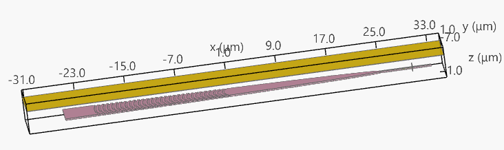
Figure 2. Exporting the layout and simulation setup to Tidy3D.
Once the simulation is run, you can visualize different field components, such as the electric field:
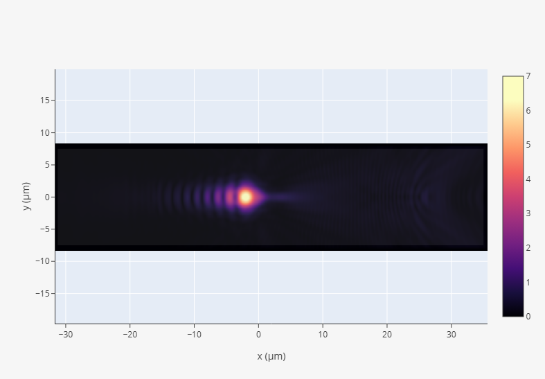
Figure 3. Distribution of the magnitude of the electric field at the field monitor specified with a setup macro.
Through the flux monitor, we also can see the power at top of the grating coupler, which equals to -3.2 dB. Now that we have performed an initial inspection of the layout and simulation setup, we are ready to optimize the grating coupler.
Sweeping the grating period to maximize out-coupled power
Note
Running this example will cost ~3.5 FlexCredits.
To optimize the grating coupler for the maximum upward coupling, we run a parameter sweep over its period and measure the power through the flux monitor. The macro for saving the result and the simulation recipe are defined below:
def flux_export():
    """
    Macro to save and return the output from a Tidy3D simulation, in this case, the flux data.

    Returns
    -------
        macro : i3.device_sim.Macro
    """

    commands = """
import tidy3d.web as web

job = web.Job(simulation=simulation, task_name="flux", verbose=True)
sim_data = job.run(path="data/simulation_data.hdf5")

with open("flux.txt", "a+") as output_file:
""".splitlines()

    write_command = '    output_file.write(f"{sim_data["flux"].flux.values[0]}\\n")'
    commands.append(write_command)

    macro = i3.device_sim.MacroOutput(name="flux", filepath="flux.txt", commands=commands)
    return macro
def simulate_gc_by_tidy3d(gc_layout, wavelength: float, neff: float, wg_w: float, h_dev: float, height: float) -> float:
    """Performs an FDTD simulation of a given grating coupler layout.
     The obtained out-coupling power is returned and saved to a file.

    Parameters
     ----------
    gc_layout : LayoutView
        Layout view of the grating coupler.
    wavelength: float
        The wavelength of the source.
    neff : float
        Effective index of the waveguide.
    wg_w: float
        Core width of the waveguide to adjust the height of the source.
    h_dev : float
        Thickness of the layer where the device is placed to adjust the height of the source.
    height : float
        Height of the monitors from top of the cladding.
    Returns
    -------
    The resulting flux at top of the simulated component.
    """
    si = gc_layout.size_info()

    simulation = i3.device_sim.Tidy3DFDTDSimulation(
        geometry=i3.device_sim.SimulationGeometry(
            layout=gc_layout,
            waveguide_growth=8,
            bounding_box=[(si.west - 6, si.east + 10), (si.south, si.north), (0, 5)],
        ),
        task_name="gc_flux",
        task_folder_name="gc_flux_optimization",
        project_folder="gc_optimized_1550_fdtd",
        setup_macros=[
            monitors(h_dev=h_dev, height=height, field=False),
            mode_source(
                alignment_port="out", neff=neff, x_port=gc_layout.ports["out"].position[0], wg_w=wg_w, h_dev=h_dev
            ),
            i3.device_sim.tidy3d_macros.fdtd_run_time(run_time=2.7e-10),
            i3.device_sim.tidy3d_macros.fdtd_auto_grid_spec(min_steps_per_wavelength=6),
        ],
        outputs=[flux_export()],
        center_wavelength=wavelength,
    )

    fpath = simulation.get_result("flux")
    return float(open(fpath).readlines()[-1])
IPKISS does not natively support exporting out-of-plane ports defined by i3.VerticalOpticalPort.
Therefore, when running this example, you will encounter a warning mentioning that the layout contains VerticalOpticalPorts ‘vertical_in’ which have to be manually implemented in the simulation software.
The warning can be ignored since we use a monitor defined via a setup macro instead of that port.
By simulating the grating coupler over a range of periods, we observe that maximum transmission at the 1.55 µm wavelength occurs at a period of 0.71 µm, as shown in the figure.
periods = np.linspace(0.65, 0.75, 6)  # Period sweep
fluxes = []

for period in periods:
    print(f"Simulating for period: {period:.2f} µm")
    gc = pdk.GratingCoupler(
        n_o_periods=30,
        socket_length=50,
        period=period,
    )
    gc_lo = gc.Layout()
    fluxes.append(simulate_gc_by_tidy3d(gc_lo, wl, neff, wg_w, h_dev=h_dev, height=height))

fig = plt.plot(periods, fluxes, marker="o")
plt.xlabel("Grating Coupler Period (µm)")
plt.ylabel("Transmission")
png_path = os.path.join("transmission.png")
plt.savefig(png_path, bbox_inches="tight")
print(f"{png_path} written")
plt.show()
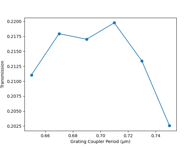
Figure 4. Transmission of the grating coupler for different values of period parameter.
Far-field projection of the grating coupler
We can also simulate the far-field projection of the grating coupler, optimized in the previous step, using a far-field monitor macro:
def far_field_monitor_xy(h_dev: float, height: float):
    """Macro to create an FDTD frequency domain Z-normal far-field monitor that covers the full simulation window,
    at a certain height.

    Parameters
    ----------
    h_dev : float
        Thickness of the layer where the device is placed.
    height : float
        Height of the monitors from top of the device.

    Returns
    -------
        macro : i3.device_sim.Macro
    """
    commands = f"""
import numpy as np
far_field_monitor_xy = td.FieldProjectionAngleMonitor(

    center=(0, 0, 1 + {h_dev} + {height}),
    size=(td.inf, td.inf, 0),
    normal_dir="+",
    freqs=[center_frequency],
    theta = np.linspace(-np.pi / 2, np.pi / 2, 1101),
    phi=[0.0],
    name="far_field",
    proj_distance=10000,
)

monitors = [far_field_monitor_xy]
"""

    macro = Macro(commands=commands.splitlines())
    return macro
The far-field monitor macro can be used in a simulation job similar to the previous examples. The far-field monitor samples the electromagnetic near fields above the grating coupler to create a far-field projection. Therefore, the monitor is placed close to the grating coupler, e.g., at a height of 100nm above the surface. The figure below is obtained by running the simulation in the luceda_academy/pdks_sources/si_fab/si_fab/ipkiss/si_fab/components/grating_coupler/doc/example_gc_sim_tidy3d/example_far_field_sim_setup.py example. From the figure we can see that the projection angle is -17 degrees.
Note
When running this simulation on the Tidy3d web GUI, you will encounter a warning mentioning that Simulation final field decay value of 0.023481 is greater than the simulation threshold of 1e-05. Consider simulation again with large run_time duration for more accurate results. To avoid this warning, you can add some setup macros—specifically, the fdtd_run_time macro—to extend the simulation duration. However, please note that increasing the run time will result in higher flex credit costs in Tidy3D.
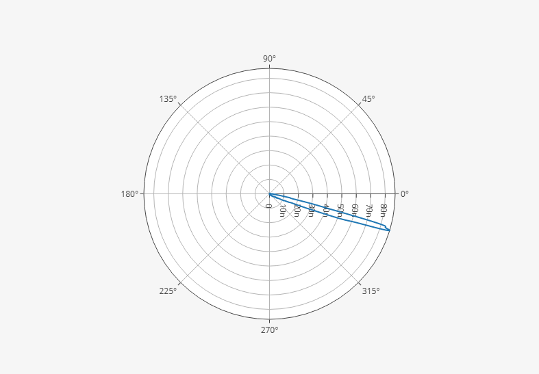
Figure 5. Far-field projection of the grating coupler.
Conclusion
In this tutorial, we demonstrated how to set up a grating coupler simulation and optimize its layout using Luceda Link for Tidy3D. We explored layout export, near-field and far-field simulations, and parameter sweeps to maximize upward coupling efficiency. The same optimization approach can be applied to grating coupler’s layout parameters other than the period.
Additionally, the simulation and optimization process can be reversed. By placing a mode source at a certain angle above the grating coupler, the parameters can be optimized for transmission at the in-plane port.
Note
The above simulation results are artificial results as they are based on a fictional technology and components. These only serve demonstration purposes.