Release notes Luceda Photonics Design Platform 2025.12.0
Welcome to the 2025.12.0 release!
Discover the key highlights:
Easy PDK creation & building - Create a new Luceda PDK with layers, component library, automated doc generation, and validation routines via a guided wizard.
Length matching - Automatically match path lengths of waveguide connectors.
Tape-out preparation - Native support for dummy filling (either directly on your IPKISS design or from GDS) and new tutorial on dealing with DRC violations (Tape-out preparation: detect and fix design rules violations).
Layout navigation and inspection - New visual aids for anchor inspection, plus cell hierarchy navigation.
Interactive signal tracer - Combine layouts and circuit simulation results in our layout viewer to debug light propagation and reflections.
Share designs easily with colleagues - Export interactive layouts and simulation results for viewing by colleagues without a Luceda license.
For a full list of features, improvements, and bug fixes, please consult the changelog.
Easy PDK creation & building
We have streamlined the process of creating a new PDK. From the Luceda Control Center, you can now launch the New Design Kit Project wizard to generate a fully structured PDK skeleton.
Quick setup: Immediately start populating your PDK with layers and library components.
Inspection: Verify your setup using the new built-in inspection routines (
ip_manager.pdk.inspect()) for layers and components.Automated build: Generate your PDK distributable with a single command (
ip_manager.pdk.build()). This automatically builds documentation (including components and trace templates), layer files (e.g., KLayout .lyp), schematic IPKISS Canvas files, and OpenAccess libraries.
Visit the following page for more information on creating and validating your IP libraries and PDKs using IP Manager: Luceda IP Manager.
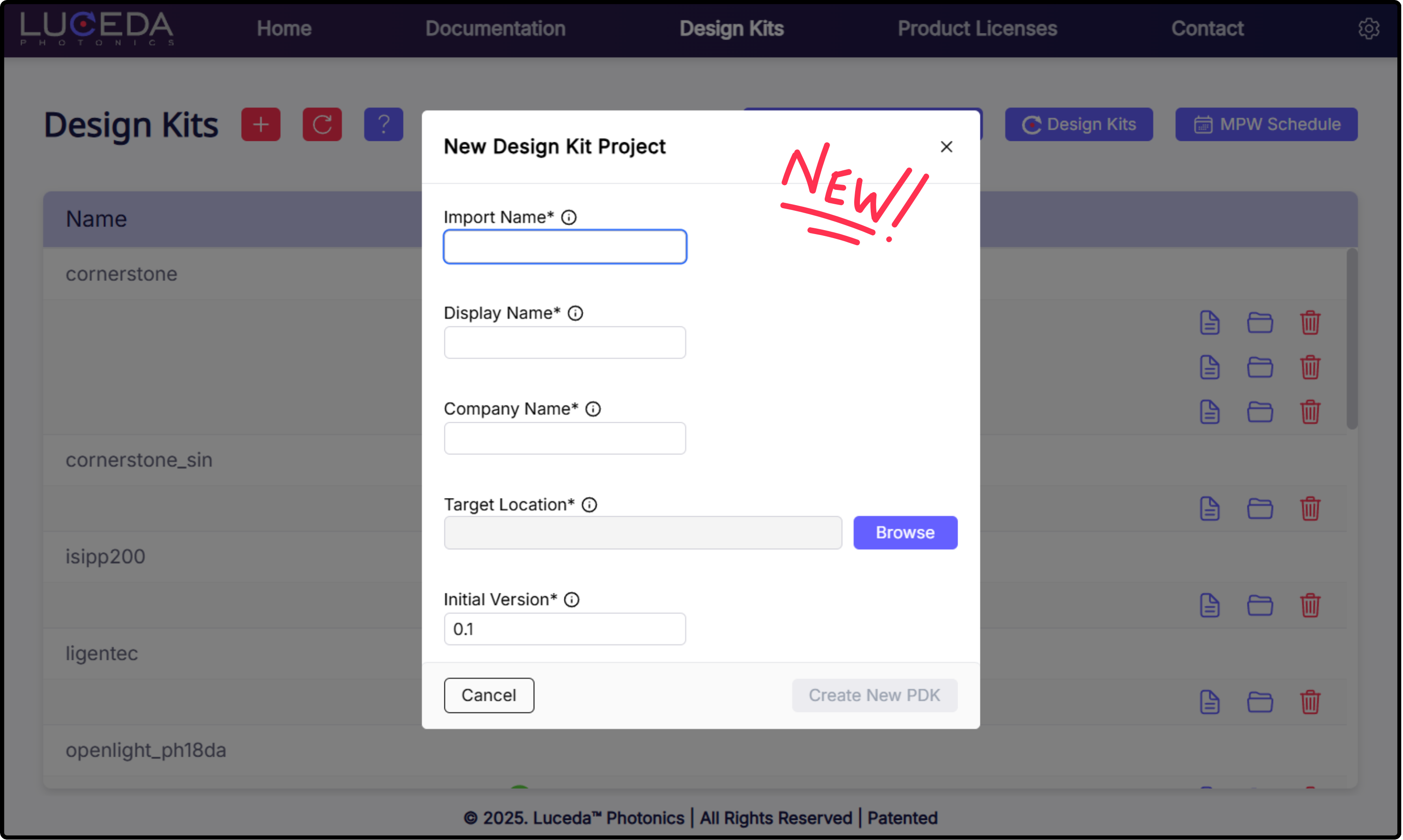
Creating a new PDK from the Luceda Control Center.
Length matching & Placement
Placement & Routing have been upgraded with two new features:
i3.MatchLength: This specification automates path length matching for Manhattan connectors by intelligently shifting control points, eliminating the need for manual tuning.i3.Distribute: A new placement specification that accepts X and Y sub-specifications (i3.Distribute.X and i3.Distribute.Y), allowing you to uniformly distribute a sequence of instances across a specific axis or grid.
Tape-out preparation
To streamline the path to manufacturing, we have introduced native dummy filling capabilities:
Layout View: Use
i3.dummy_fill_layoutto apply fill directly to an IPKISS Layout while designing.GDSII: Use
i3.dummy_fill_gdsiito post-process existing GDSII files.
In addition, we have added a new tutorial about preparing your design for tape-out at the following link: Tape-out preparation: detect and fix design rules violations.
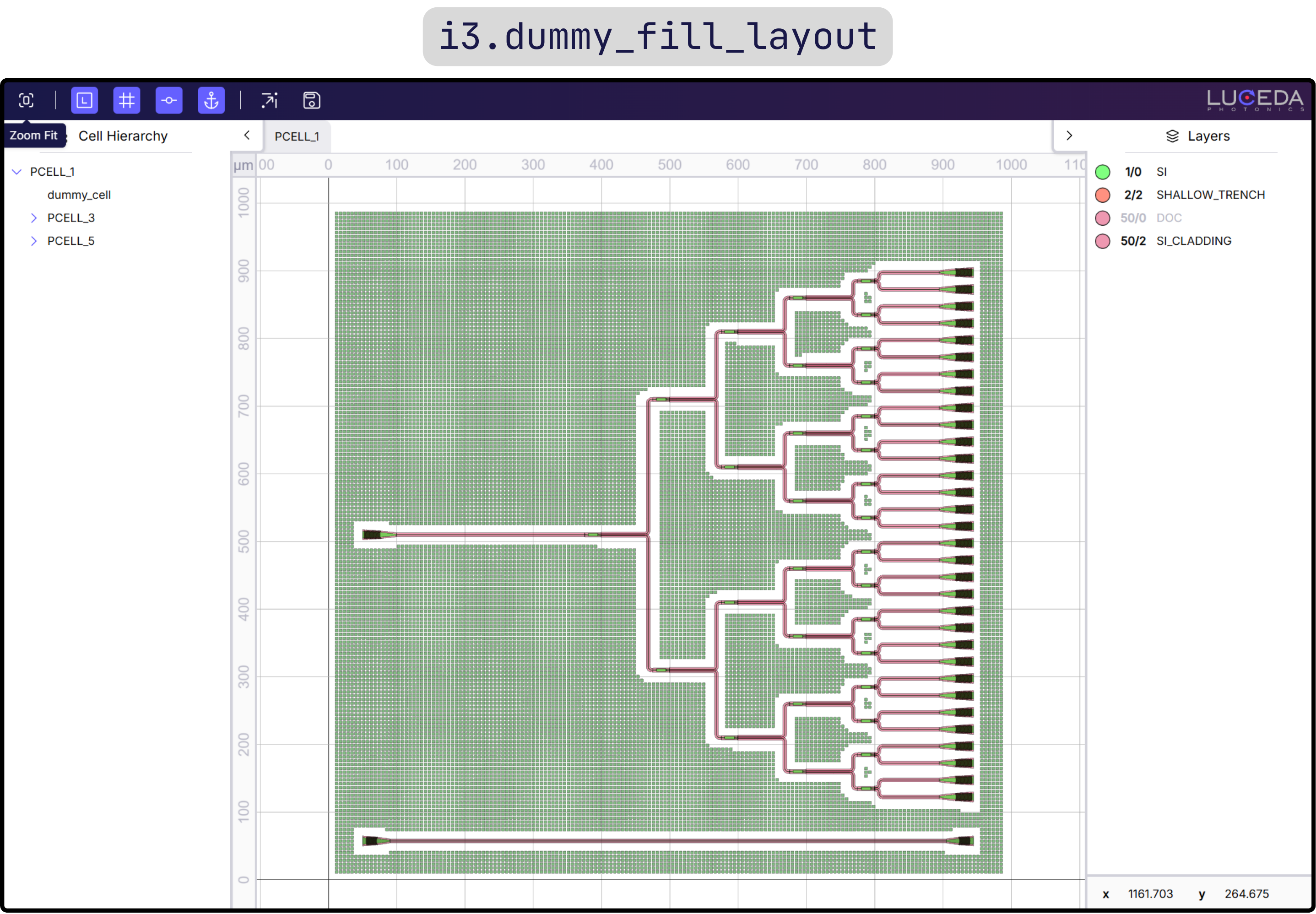
Dummy filling a layout using the new Luceda dummy filling functionality.
Layout navigation and inspection
The layout visualizer has been updated to support new navigation and inspection features, useful during layout design:
Anchor visualization: User-defined anchors created with
i3.Anchorare now rendered in the visualizer, when clicking on an instance. This way, you can easily copy the instance (inst) and anchor (inst@anchor) names for direct use in your P&R code.Hierarchy navigation: You can now view and navigate the full cell hierarchy and toggle visibility for individual cells or layers to isolate specific parts of your circuit.
Visual UX improvements: We improved zoom behavior for grids/axes and fixed highlighting bugs where hidden layers would react to mouse hovers.
In addition, we have added a new tutorial about preparing your design for tape-out at the following link: Tape-out preparation: detect and fix design rules violations.
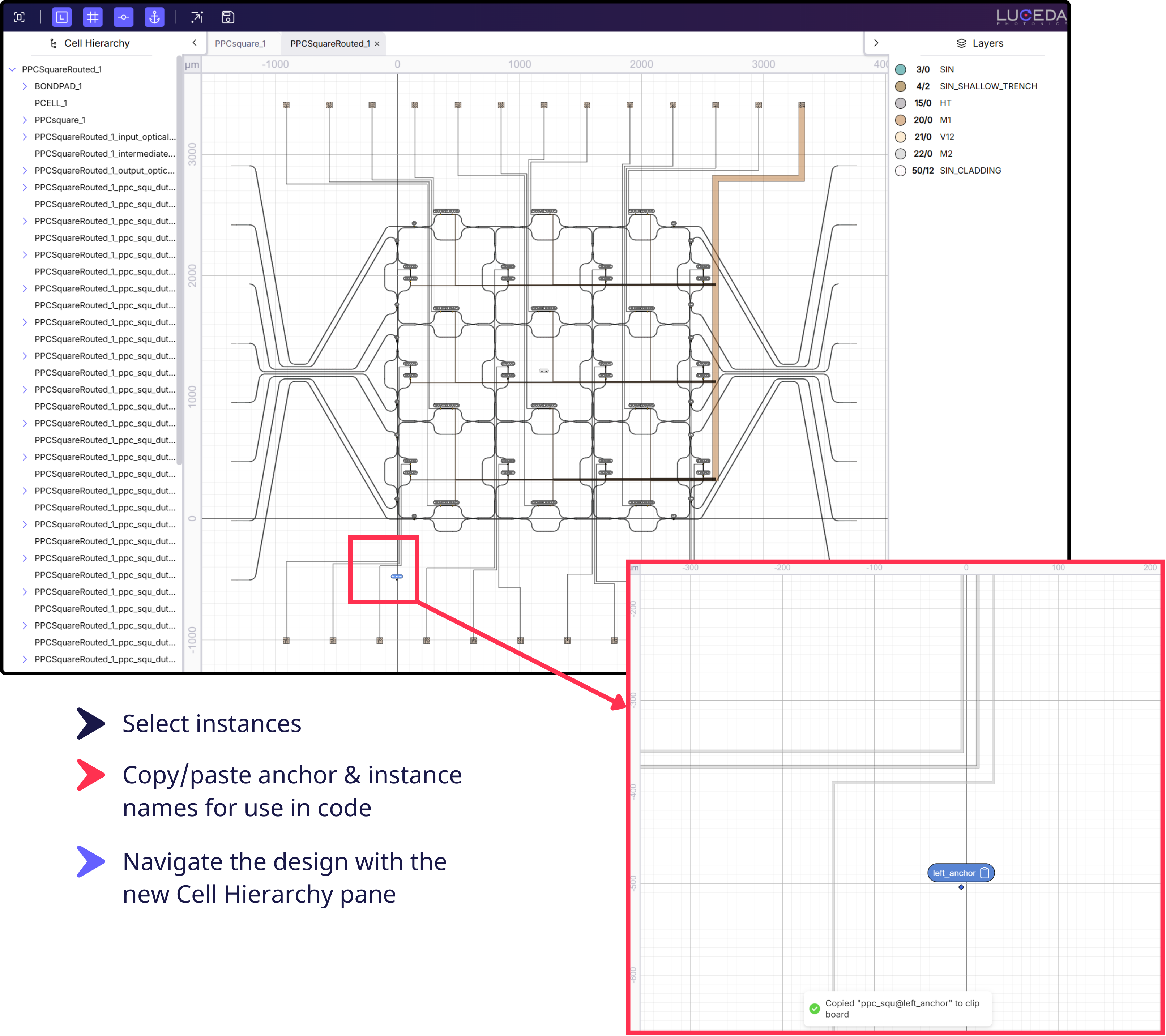
Navigating and inspecting a PIC layout with the new cell hierarchy and anchor visualization features.
Interactive signal tracer
We are excited to introduce the Signal Tracer, a tool that allows you to view PIC designs and simulation results simultaneously. This feature provides immediate insight into how signals propagate through your circuit, offering a clear visualization of major loss mechanisms and wavelength dependence.
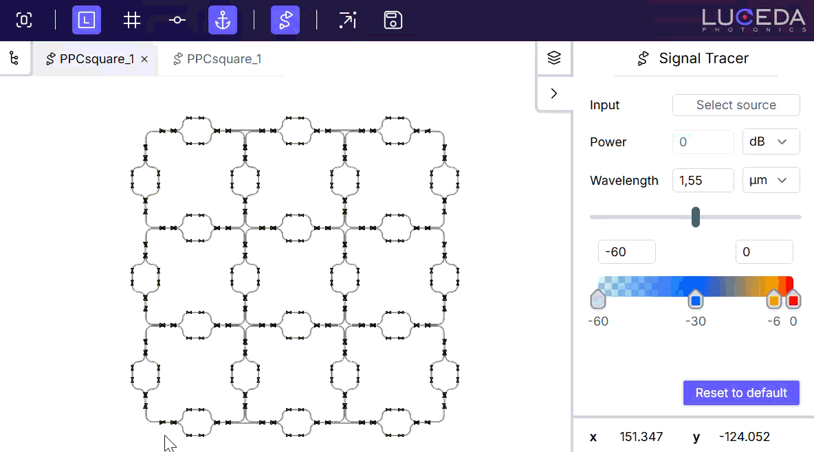
Interactive Signal Tracer showing layout + simulation.
Simulation robustness
We have improved the robustness of the simulation engine to help you get results faster:
Mixed-Mode Support: Fixed issues preventing simulations containing a mix of multimode and single-mode devices.
Remove Undefined Models From Circuit Simulation: When models are undefined or cannot evaluate, they are removed from the simulation netlist prior to simulation. This is mostly useful when there are electrical devices without model that do not contribute to the optical simulation. Warnings are given in case models cannot be netlisted.