Release notes Luceda Photonics Design Platform 2025.09.0
Welcome to the Luceda Photonics Design Platform 2025.09.0 release!
Discover the key highlights:
Interactive S-matrix Visualizer - Interactively inspect frequency-domain simulation results - select different ports pairs, toggle linear/log scales, customize plots styling, export to images or interactive HTML.
Immersive layout - Interactive layout viewer with live reloading, tabs, and instance inspection.
New P&R features - Electrical routing with 45-degree corners and new custom & cardinal anchors.
Sharp angles and layer overlaps detection - Enhanced sharp angles and layer overlaps detection and visualization.
LVS flow - Introduction of an LVS (Layout vs Schematic) flow with a supporting tutorial.
Circuit Analyzer improvements - Variability-aware waveguide models in SiFab and several samples to illustrate how Circuit Analyzer works. A new Circuit Analyzer configuration editor directly from IPKISS Canvas.
New PDK layer creation flow - A simplified workflow for defining PDK layers using
tech.yaml.
For a full list of features, improvements, and bug fixes, please consult the changelog.
Interactive S-matrix Visualizer
Visualizing S-matrix results will use the new Luceda S-matrix Visualizer. This means you no longer need to rerun your scripts each time you want to update plotting configurations, so you can focus on exploring the simulation results. Options through the Python API (such as which port pairs to select for plotting) are passed to the new visualizer as well.
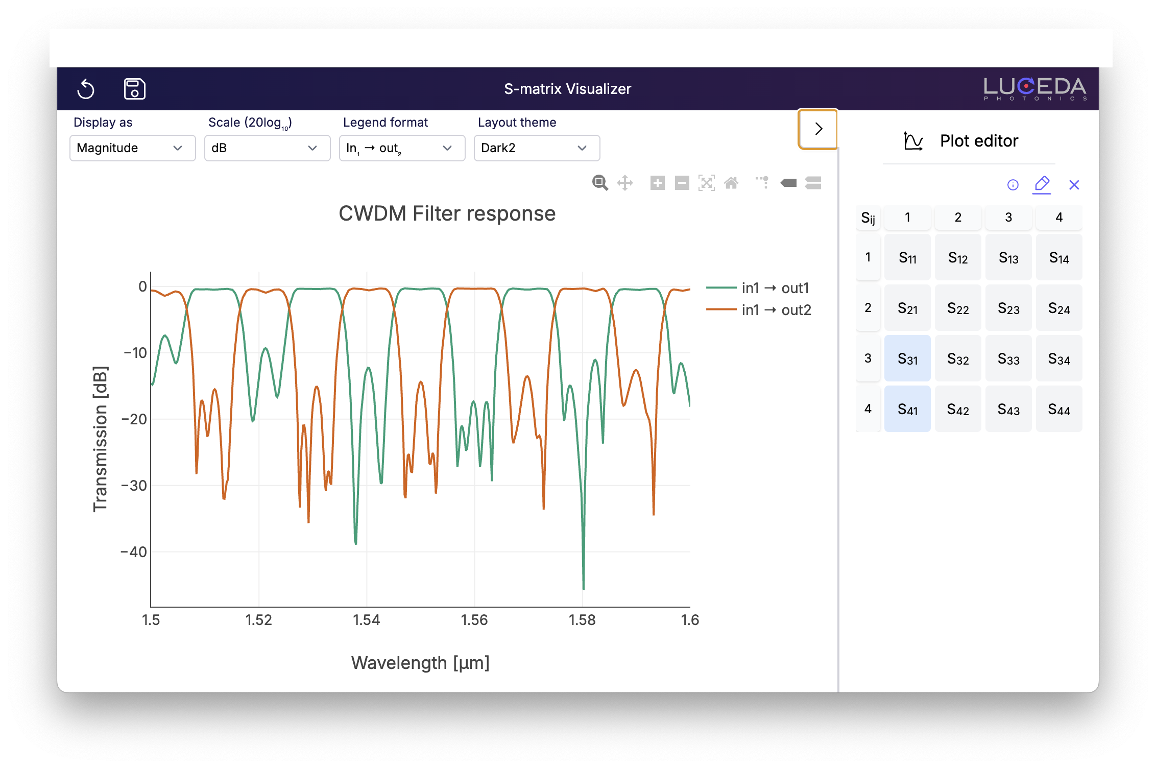
New S-matrix Visualizer, showing the result of a C-band CWDM filter.
Once you’ve customized your plots by selecting the relevant curves and preferred styling, you can save the plot to a variety of outputs. such as a static image or HTML. The HTML is still interactive after saving to disk, and allows to zoom in/out, select plots from the legend and so on. This enables you to share simulation results with colleagues easily.
Immersive layout
We’ve updated the behaviour of the Luceda Layout Visualizer (available as of the 2025.06 release), enabling a much faster and more immersive workflow:
Multiple
.visualize()calls within the same script now open as tabs in a single window rather than in separate windows.Re-running a script will automatically reload the view in the corresponding tab, rather than opening a new window.
To further assist you during placement and routing (P&R), you can now click an instance to zoom in on it.
You can also easily copy the instance (inst) and port (inst:port) names for direct use in your code.
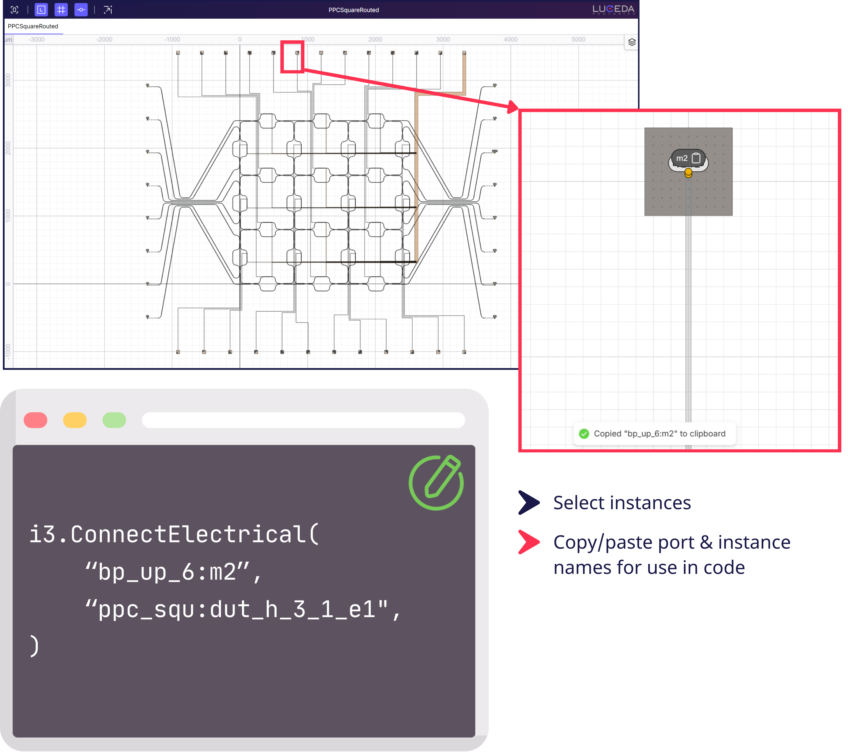
Interacting with instances and ports in an IPKISS Layout.
New P&R features
New capabilities have been added for electrical routing and the definition of placement anchors.
Electrical routing with 45-degree corners: It is now possible to add 45-degree corners to 90-degree bends in electrical traces. To enable this, set the
chamfer_lengthargument oni3.ConnectElectricalori3.ConnectElectricalBundleto a floating point value greater than 0. The trace will be chamfered with a centerline length equal to the provided value. This helps reduce the circuit footprint, improve current density uniformity, and improve fabrication yield.
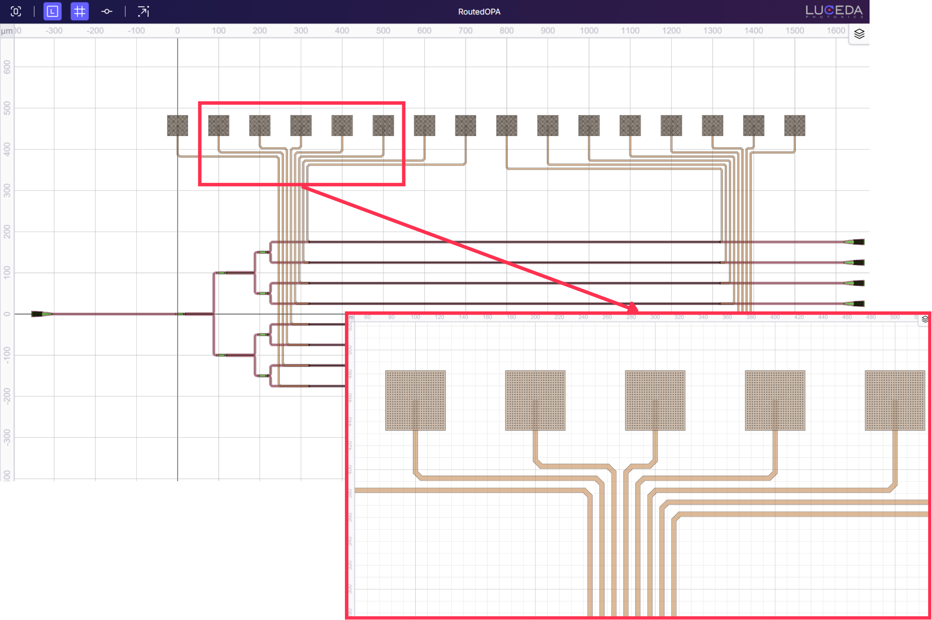
Electrical connector with 45-degree corners.
Custom anchors: The new
i3.Anchorcan be used to define custom anchors inside a PCell layout. These anchors serve as virtual reference points for placement and routing that do not correspond to a physical port.New cardinal anchors: Four new default cardinal anchors are now available on any cell: CN (Center-North), CS (Center-South), CE (Center-East), and CW (Center-West). These are automatically available on every cell and can be used as P&R references. See Symbols for more information.
DRC
The layout visualizer can now display the output of i3.get_acute_angle_points and i3.get_layer_overlaps.
Visualizing the violation markers generated by these functions helps you locate and fix DRC errors.
For reference please check visualizing violations.
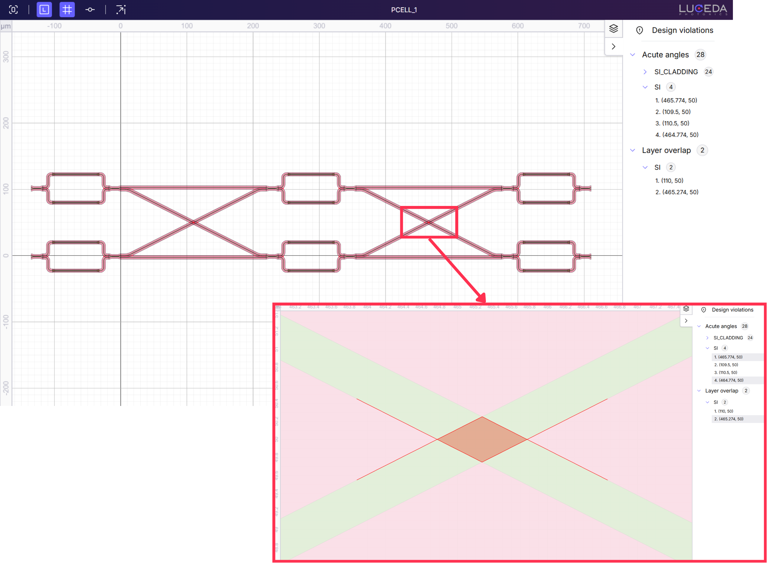
Detecting and visualizing acute angles and layer overlaps.
LVS flow
A new LVS flow has been enabled in IPKISS.
This verification feature allows you to directly compare your Canvas schematic with the GDS layout file created from IPKISS code, helping you catch potential discrepancies between design intent and implementation.
The newly added i3.run_lvs function automatically extracts the netlists from the provided Canvas schematic and GDS layout, and provides a report of the differences.
To get you started, a new tutorial is available that guides you step-by-step through this important verification process: Layout versus Schematic (LVS).
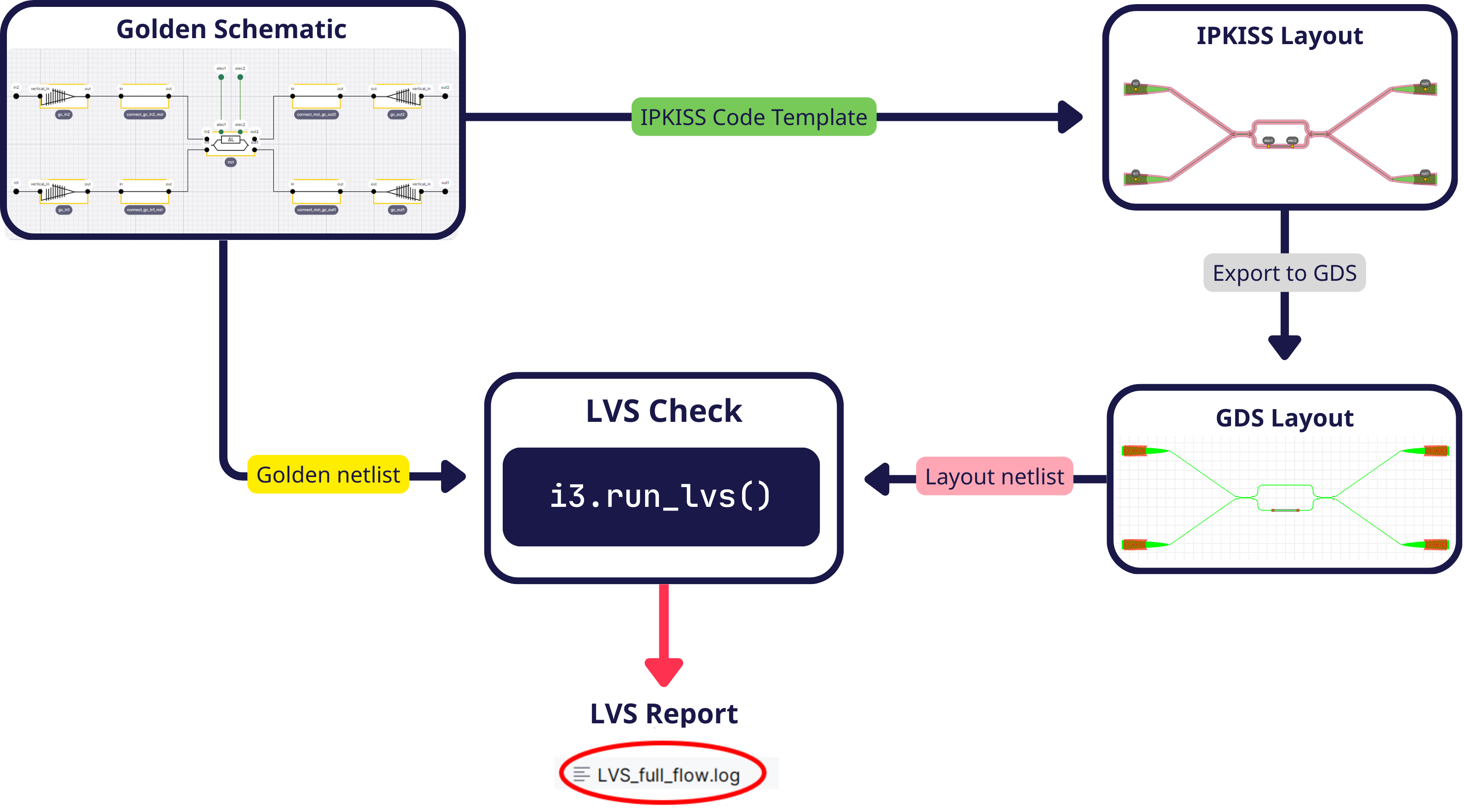
LVS flow in Luceda IPKISS.
Circuit Analyzer improvements
Circuit Analyzer configuration editor
To simplify the setup of Circuit Analyzer, you can now directly edit the configuration files from IPKISS Canvas. In addition, the simulation configuration format has been improved - see changelog for more details and the backward compatibility notes.
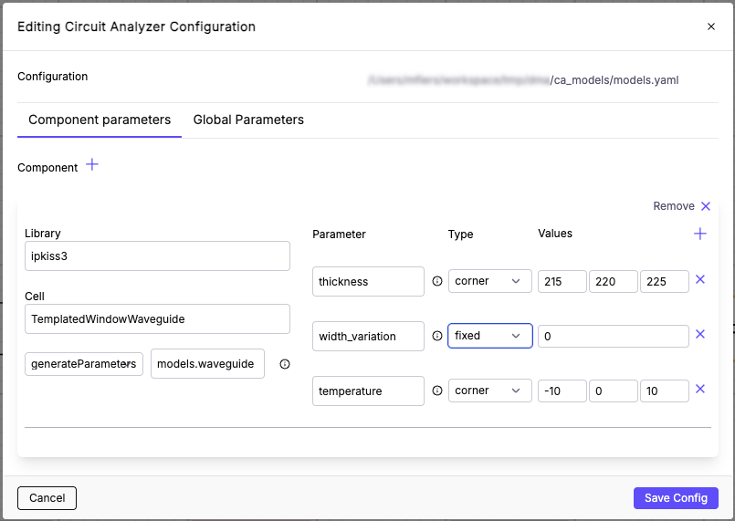
Configuring Circuit Analyzer from IPKISS Canvas (after adding a Corner Analysis codelet)
Together with the new S-matrix visualizer, this enables a full graphical workflow in IPKISS Canvas:
edit corners (i.e., to test different assumptions / edge cases),
run simulation,
interactively inspect results,
repeat.
Circuit Analyzer in Luceda Academy
To demonstrate Circuit Analyzer, several improvements are made in this release.
Waveguide model of SiFab can now interpolate n_eff as function of width and height of the waveguide, hence making it variability-aware.
New demonstrations: Location Aware Variability Analysis (
samples/circuit_analyzer/ring_demux_analysis) and Corner Analysis (samples/circuit_analyzer/waveguide_variability).New examples in the sample gallery: Location Aware Variability Analysis of a demultiplexer and Corner and Power Budget Analysis of MUX Devices.
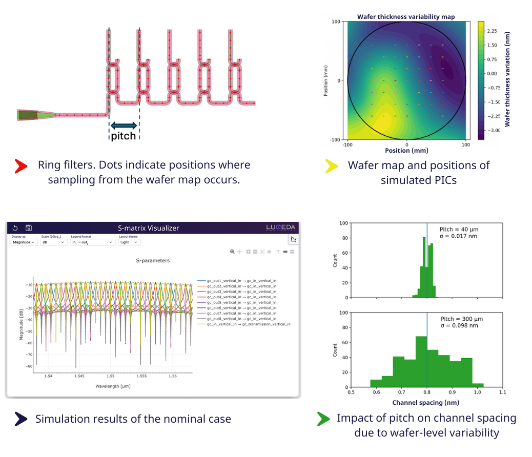
Example on Location-Aware Variability Analysis - impact of the pitch between rings on the channel spacing variability.
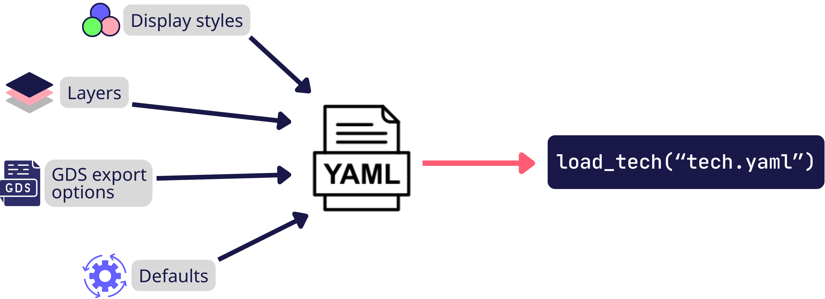
New PDK layer creation flow
The process for defining PDK layers has been refactored for simplicity and clarity.
All layer-related settings are now specified in a single, human-readable configuration file: tech.yaml.
Once loaded using load_tech(), this file is automatically used by IPKISS.
This means less boilerplate code and a clearer definition for your entire technology stack.
For more information, please refer to the following tutorial: PDK structure.
New PDK layer setup flow.