Tape-out preparation: detect and fix design rules violations
The introduction to this tutorial series highlighted several common DRC issues. In what follows, we demonstrate how these violations can be detected and resolved using Luceda’s powerful verification functionalities.
Detection and inspection
Depending on the level of detail required for checking design rules, you can choose between:
1. DRC:
It is an integrated DRC engine that provides a thorough inspection of a photonic integrated circuit (PIC) layout against foundry-provided rule decks. This ensures that your design strictly adheres to the manufacturing constraints of your chosen PDK.
To learn more about the capabilities of this powerful engine please have a look at the DRC tutorial.
Note
DRC requires a specific license. Contact us if you are interested in a trial!
2. General geometry checks:
IPKISS provides built-in tools to detect common layout “red flags” like overlapping layers and acute angles. These functionalities are included in the standard IPKISS installation and help catch errors that could lead to fabrication failure. It is good to keep in mind that these are general detection tools and that these checks are not tied to a specific fabrication process of a foundry.
In particular, these tools allow you to detect:
Overlapping layers: Finding areas where elements intersect in ways that might lead to shorts or unexpected optical behavior.
Acute angles: Identifying “sharp” geometry that is difficult for lithography tools to resolve accurately.
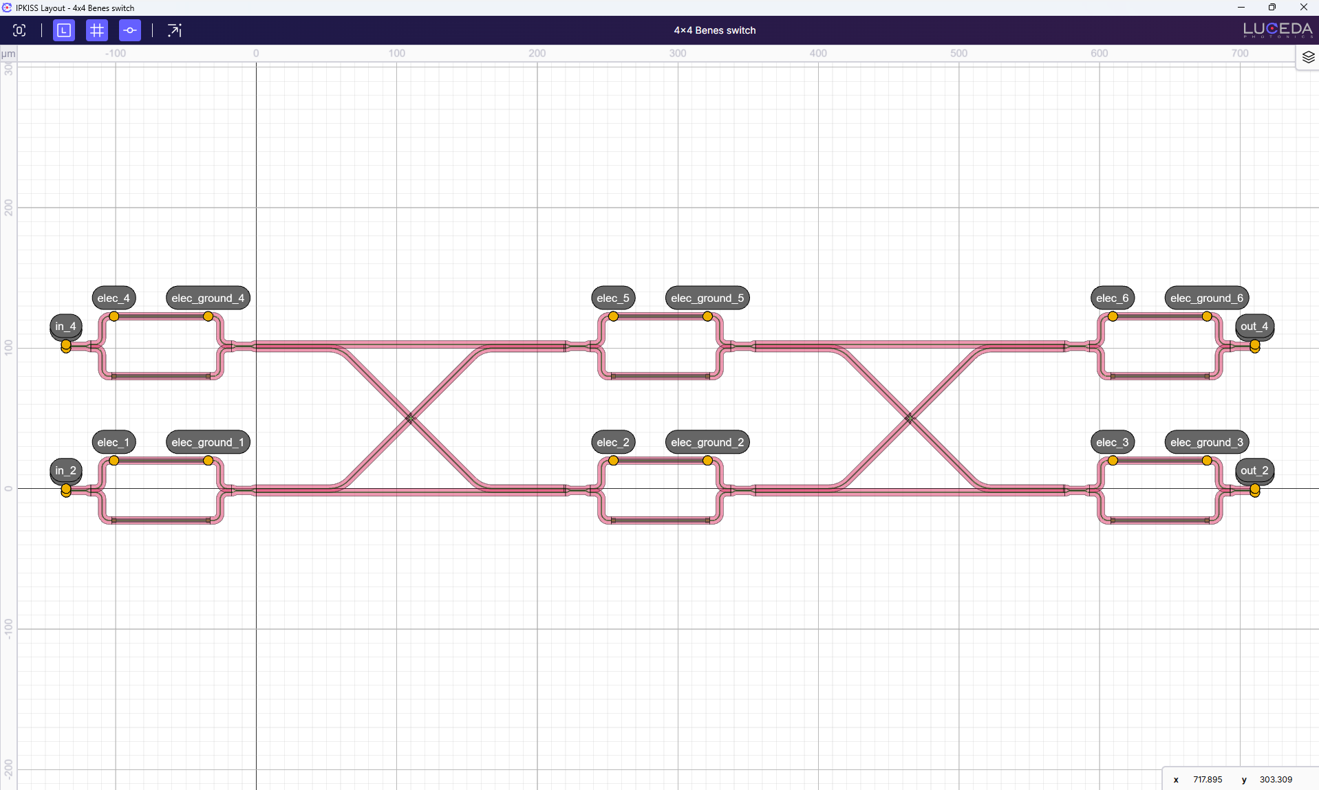
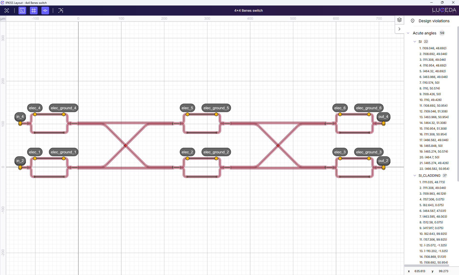
In the following subsections, we will use these checks to detect overlapping layers and acute angles in a 4x4 Benes switch architecture. A Benes network is a type of multistage interconnection network that is used for connecting multiple inputs to multiple outputs. It is considered a non-blocking network, which means that a path for a new connection can always be found without having to block an existing one.
Overlapping layers
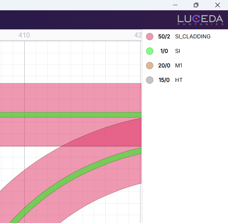
Unintended overlaps are a DRC issue as they might cause bad or unpredictable results during processing. This type of mistake can easily be missed by a designer as the layer rules are not always violated when this happens.
The 4x4 Benes switch can connect any of its four input ports to any of its four output ports without disrupting other connections. The waveguide crossings are a fundamental and indispensable part of the architecture. They are what allow the top row of switches to connect to the bottom row, enabling the non-blocking functionality that defines the Benes architecture.
To understand this circuit better, let’s first inspect the code.
class Switch4x4_Benes(i3.Circuit):
    switch = i3.ChildCellProperty(doc="2x2 MZI switch.")
    crossing = i3.ChildCellProperty(doc="Crossing.")
    spacing_x = i3.PositiveNumberProperty(default=220, doc="Spacing in x direction.")
    spacing_y = i3.PositiveNumberProperty(default=100, doc="Spacing in y direction.")
    vbias = i3.ListProperty(doc="DC bias values applied to the heater of each MZI.")

    def _default_vbias(self):
        # bar config
        return [2.416, 2.416, 2.416, 2.416, 2.416, 2.416]

    def _default_switch(self):
        return Switch_MZI2x2()

    def _default_crossing(self):
        crossing = pdk.Crossing(segment_length=0.3748)
        return crossing

    def _default_specs(self):
        specs = []
        for i in range(len(self.vbias)):
            inst_name = f"s{i // 3}_{i % 3}"
            specs.append(i3.Inst(name=inst_name, reference=self.switch.modified_copy(vdiff=self.vbias[i])))
        specs += [
            i3.Place("s0_0:out_2", (0, 0)),
            i3.Place("s0_1:in_2", (self.spacing_x, 0), relative_to="s0_0:out_2"),
            i3.Place("s1_0:out_1", (0, self.spacing_y), relative_to="s0_0:out_2"),
            i3.Place("s1_1:in_1", (self.spacing_x, self.spacing_y), relative_to="s0_0:out_2"),
            i3.Place("s0_2:in_2", (self.spacing_x, 0), relative_to="s0_1:out_2"),
            i3.Place("s1_2:in_2", (self.spacing_x, 0), relative_to="s1_1:out_2"),
            i3.ConnectBend(
                [
                    ("s0_0:out_1", "s0_1:in_1"),
                    ("s0_1:out_1", "s0_2:in_1"),
                    ("s1_0:out_2", "s1_1:in_2"),
                    ("s1_1:out_2", "s1_2:in_2"),
                    ("s0_0:out_2", "s1_1:in_1"),
                    ("s1_0:out_1", "s0_1:in_2"),
                    ("s0_1:out_2", "s1_2:in_1"),
                    ("s1_1:out_1", "s0_2:in_2"),
                ],
                start_straight=5,
                end_straight=5,
                bend_radius=25,
            ),
        ]
        return specs
Let’s inspect the circuit to see if there are layer overlaps present.
To do this in IPKISS we can use .visualize_violations(acute_angle_layers=[], overlap_layers=[i3.TECH.PPLAYER.SI]).
We pass an empty list to acute_angle_layers as at this point we are only interested in layer overlap.
if __name__ == "__main__":  # this line means the enclosed code will only run if this file is run directly
    switch = Switch4x4_Benes()
    lv = switch.Layout(name="4x4_benes_switch")
    lv.visualize()
    lv.write_gdsii("4x4.gds")

    # overlapping layer detection
    lv.visualize_violations(acute_angle_layers=[], overlap_layers=[i3.TECH.PPLAYER.SI])
This method identifies and highlights overlapping sections on specified physical layers. The visualization appears directly on your layout in the Luceda Layout Visualizer.
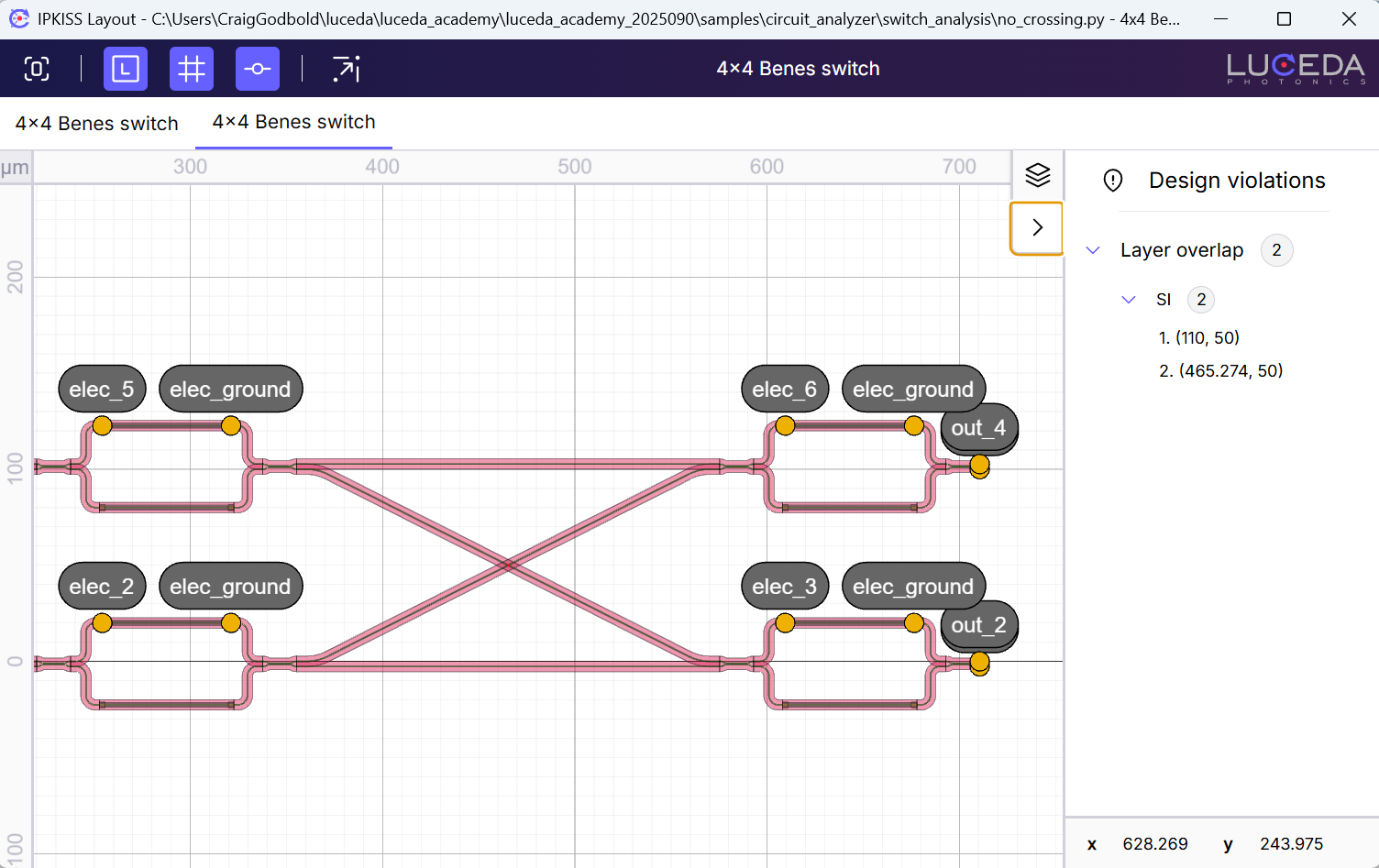
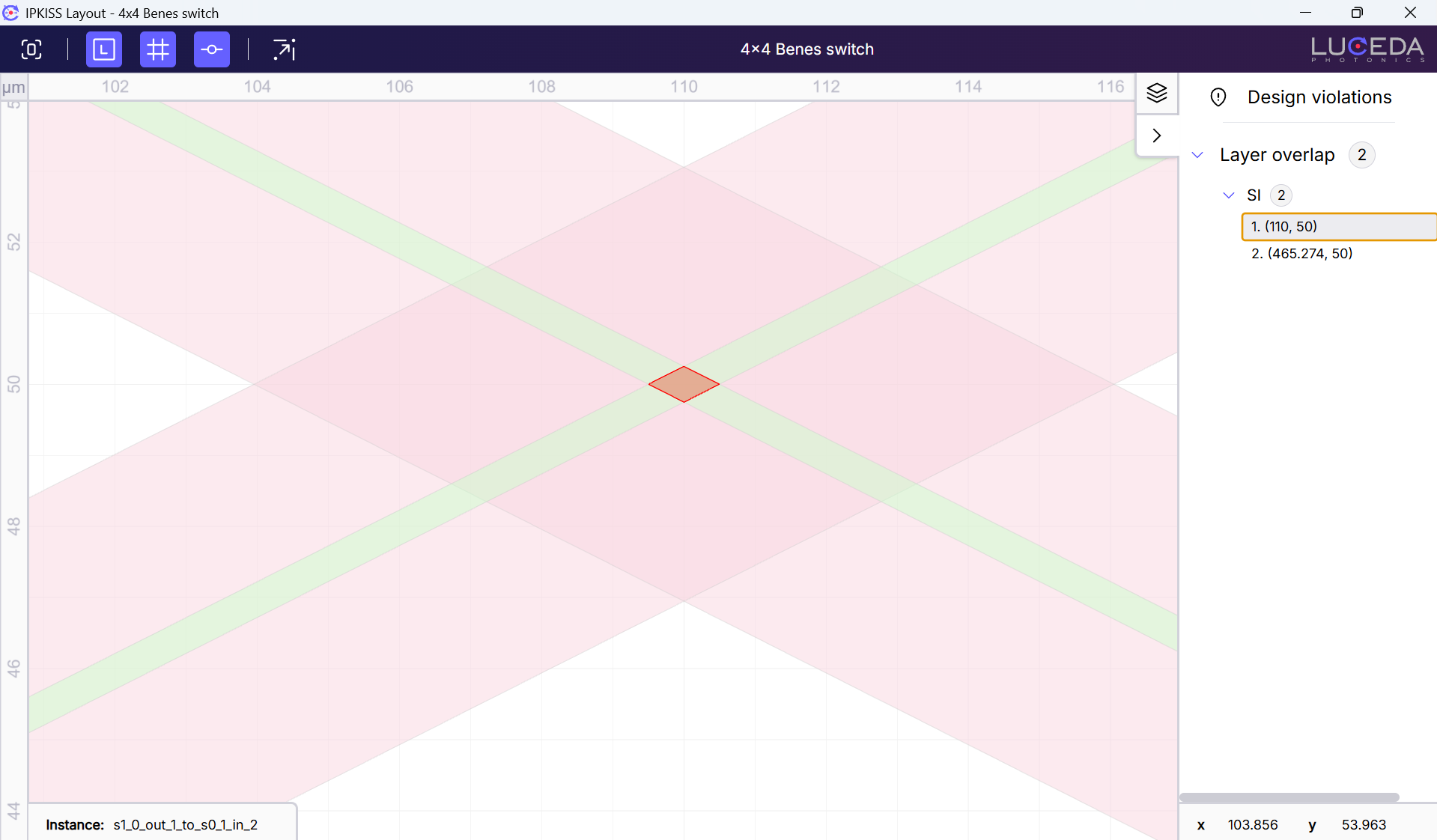
A quick analysis of our circuit code indicates that a mistake has been made in the circuit’s instances dictionary and specs list. The waveguide crossings are not appearing in the final layout. Although a crossing PCell was defined in the class parameters, it was never added to the circuit’s instances and specifications (insts and specs).
It is now a simple case of adding the crossing into the layout correctly by amending the insts and specs.
    def _default_specs(self):
        specs = []
        # Here we create all instances (components) of the circuit.
        # Loop to create and name the six 2x2 switches.
        for i in range(len(self.vbias)):
            # The instance name is generated dynamically (e.g., "s0_0", "s0_1", etc.).
            inst_name = f"s{i // 3}_{i % 3}"
            # A new switch instance is created with its vdiff property set.
            specs.append(i3.Inst(name=inst_name, reference=self.switch.modified_copy(vdiff=self.vbias[i])))

        # Here we specify the details concerning the placement and routing of all components.
        specs += [
            # Explicitly create instances of the crossings as they are not part of the loop.
            i3.Inst(["c1", "c2"], self.crossing),
            # SWITCH PLACEMENT - Place the s0_0 switch at the origin (0,0) of the layout.
            i3.Place("s0_0:out_2", (0, 0)),
            # Place the remaining switches relative to the s0_0 switch to create the grid.
            i3.Place("s0_1:in_2", (self.spacing_x, 0), relative_to="s0_0:out_2"),
            i3.Place("s1_0:out_1", (0, self.spacing_y), relative_to="s0_0:out_2"),
            i3.Place("s1_1:in_1", (self.spacing_x, self.spacing_y), relative_to="s0_0:out_2"),
            i3.Place("s0_2:in_2", (self.spacing_x, 0), relative_to="s0_1:out_2"),
            i3.Place("s1_2:in_2", (self.spacing_x, 0), relative_to="s1_1:out_2"),
            # CROSSING PLACEMENT - Place the crossings at the center of the grid squares.
            i3.Place("c1@C", (self.spacing_x / 2, self.spacing_y / 2), relative_to="s0_0:out_2"),
            # Rotate the crossing by 45 degrees to allow diagonal routing.
            i3.Place.Angle("c1", 45),
            i3.Place("c2@C", (self.spacing_x / 2, self.spacing_y / 2), relative_to="s0_1:out_2"),
            i3.Place.Angle("c2", 45),
            # Use ConnectBend to automatically draw waveguides between the specified ports.
            i3.ConnectBend(
                [
                    # Straight connections between switches in the same row/column.
                    ("s0_0:out_1", "s0_1:in_1"),
                    ("s0_1:out_1", "s0_2:in_1"),
                    ("s1_0:out_2", "s1_1:in_2"),
                    ("s1_1:out_2", "s1_2:in_2"),
                    # Connections involving the crossings to create the Benes architecture.
                    ("s0_0:out_2", "c1:in1"),
                    ("s0_1:in_2", "c1:in2"),
                    ("s1_0:out_1", "c1:out2"),
                    ("s1_1:in_1", "c1:out1"),
                    ("s0_1:out_2", "c2:in1"),
                    ("s0_2:in_2", "c2:in2"),
                    ("s1_1:out_1", "c2:out2"),
                    ("s1_2:in_1", "c2:out1"),
                ],
                # Now all connections will have the same straight sections
                start_straight=10,  # You can adjust this value
                end_straight=10,  # You can adjust this value
                bend_radius=20,
            ),
        ]
        return specs
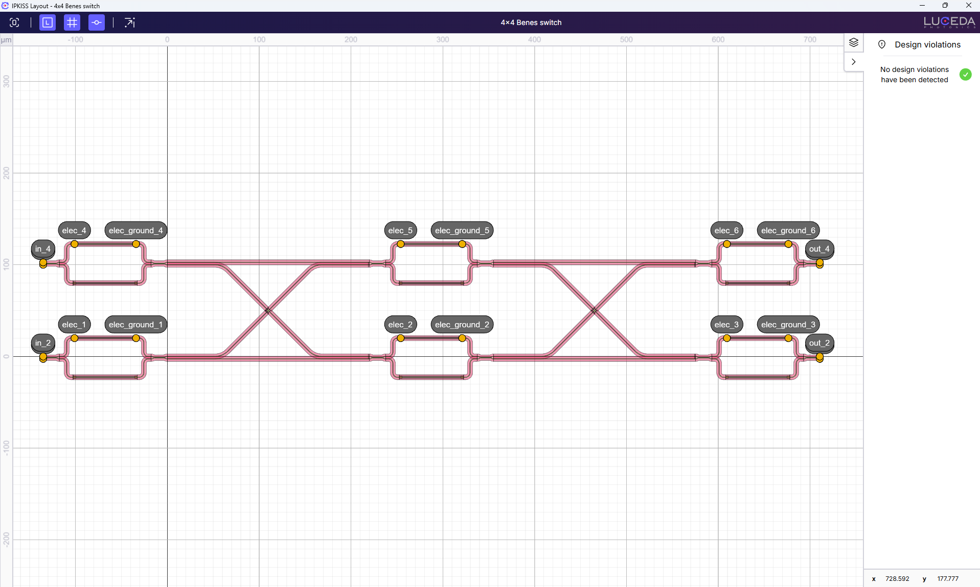
With the crossing correctly placed in the circuit, we no longer see overlapping layers detected!
Acute angles
Foundries often impose strict rules on the sharpness of angles in PIC designs to ensure compatibility with lithographic and etching processes. IPKISS has several built-in functions that allow designer to both detect and fix all acute angles in the design.
When zooming in on different locations of our 4×4 Benes switch, we can observe by visual inspection that acute angles are present.
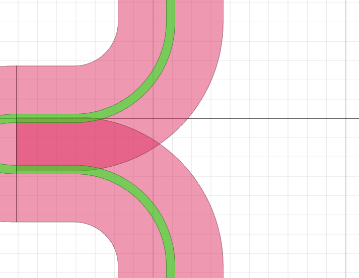
However, the process of manually inspecting a design is highly inefficient and these angles are not always noticeable by visual inspection.
Let’s simplify this process by using the built-in functionality of IPKISS to automatically detect all acute angles in the circuit.
We achieve this by using .visualize_violations(overlap_layers=[]).
We pass an empty list to overlap_layers as at this point we are only interested in acute angles.
Here is an example of how to use this method:
if __name__ == "__main__":  # this line means the enclosed code will only run if this file is run directly
    switch = Switch4x4_Benes(name="4x4_benes_switch")
    lv = switch.Layout()
    lv.visualize()
    lv.write_gdsii("4x4.gds")

    # Overlapping layer detection
    lv.visualize_violations(acute_angle_layers=[], overlap_layers=[i3.TECH.PPLAYER.SI])

    # Acute angle detection
    lv.visualize_violations(overlap_layers=[])
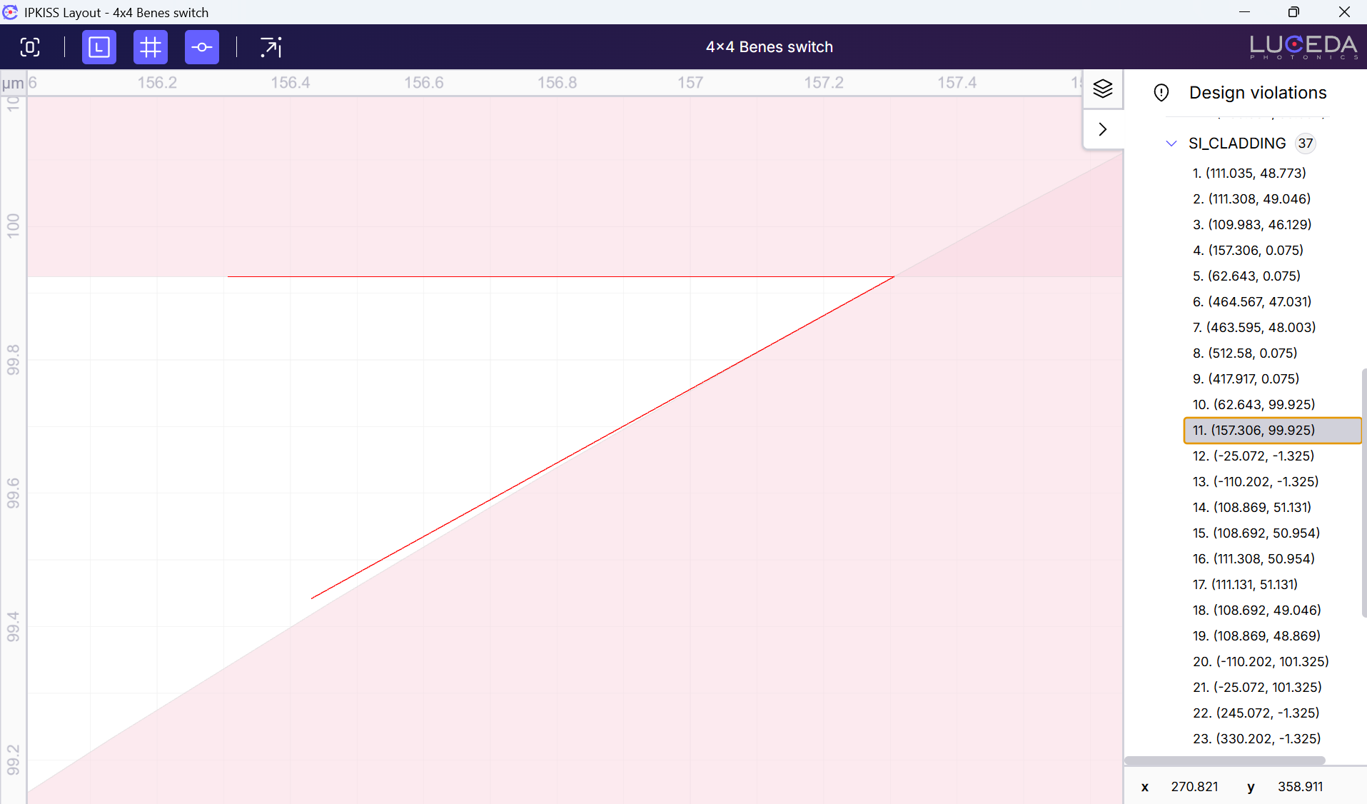
The visualize_violations will analyze the entire layout (all layers) for acute angles if the acute_angles_layers list is not provided. This method detects angles less than 90° or greater than 270°.
We can now easily inspect the acute angles in the visualizer:
Fixing design errors
Once violations are detected, you can use IPKISS functionalities to fix the errors until you reach a DRC clean design. Most issues such as bend radii or metal widths can be resolved instantly by tweaking your design parameters. For other geometry hurdles like acute angles or snapping errors, IPKISS provides intelligent automation to clean up your layout for you. In the following subsections, you can learn how to fix acute angles and snapping errors with IPKISS functionality.
Acute angles
Acute angles can easily be fixed by applying a stubbed element.
To do this, we use i3.get_stub_elements().
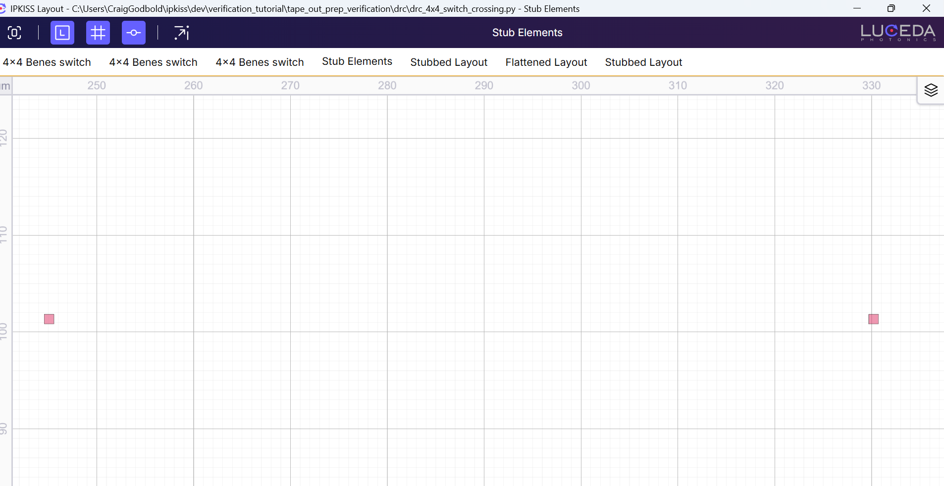
Before adding the stubbed elements to a new circuit layout, we can inspect them without the rest of the circuit.
    # Define a custom LayoutView to apply the stubbing automatically
    acute_angle_collection = i3.get_acute_angle_points(lv, layers=[pdk.TECH.PPLAYER.SI_CLADDING])
    acute_angle_points = [angle_point[0] for angle_point in acute_angle_collection[pdk.TECH.PPLAYER.SI_CLADDING]]
    stub_elems = [
        i3.Box(layer=pdk.TECH.PPLAYER.SI_CLADDING, center=acute_angle_point, box_size=(1, 1))
        for acute_angle_point in acute_angle_points
    ]

    stubs_lay = i3.LayoutCell(name="stub_elements").Layout(elements=stub_elems)
    stubs_lay.visualize()
This section of code defines a custom LayoutView to apply the stubbing automatically. It detects acute-angle points in the silicon cladding layer and creates small 1×1 µm stubs centered on each location. These stubs are then assembled into a simple layout cell for visualization.
The output of stubs_lay.visualize() gives us the elements that will be added to the full layout.
The next step is to merge those stubs back into the original layout, producing a new stubbed layout.
    # Stub the acute angles and create a new layout
    layout_elements = i3.get_layer_elements(lv)
    layers = list(set([el.layer for el in layout_elements]))
    stubbed_elements = i3.merge_elements(layout_elements + stub_elems, layers=layers)

    stubbed_layout = i3.LayoutCell(name="stubbed_layout").Layout(elements=stubbed_elements, ports=lv.ports)
    stubbed_layout.visualize()
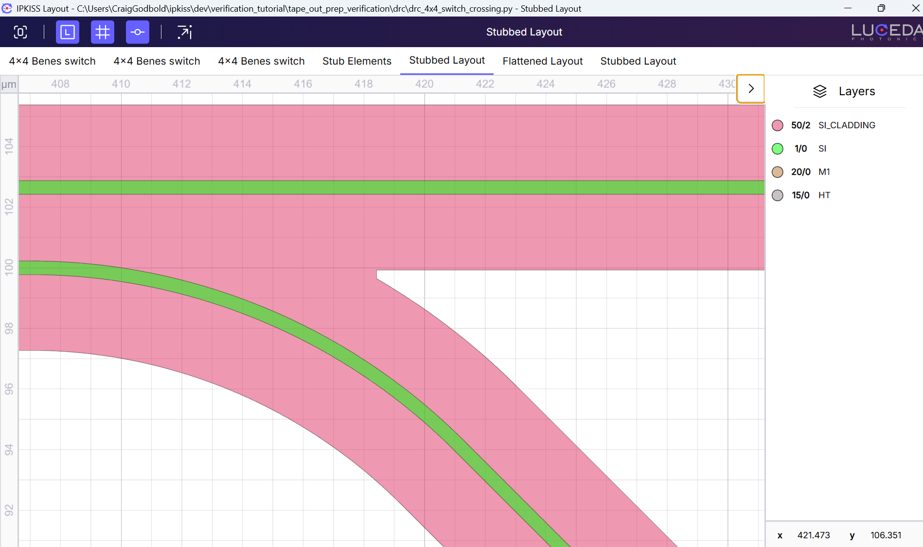
The new layout has no acute angle violations!
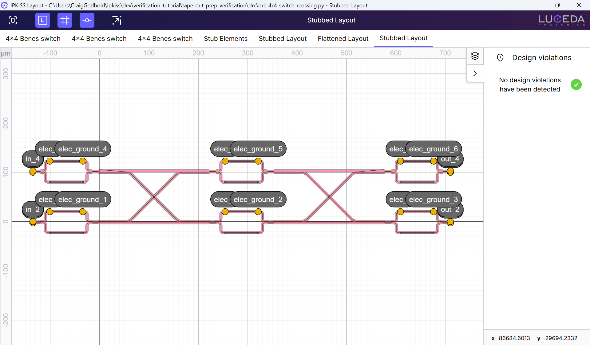
Note
The .visualize_violations() by default does both the overlap layer and acute angle detection as can be seen in this code example.
    # visualize_violations method by default does both acute angle & overlapping layer detection
    stubbed_layout.visualize_violations()
Snapping errors
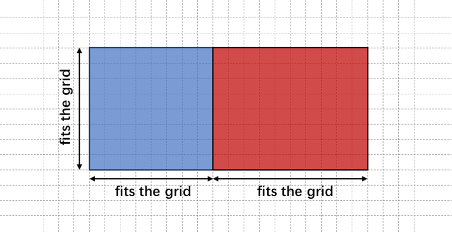
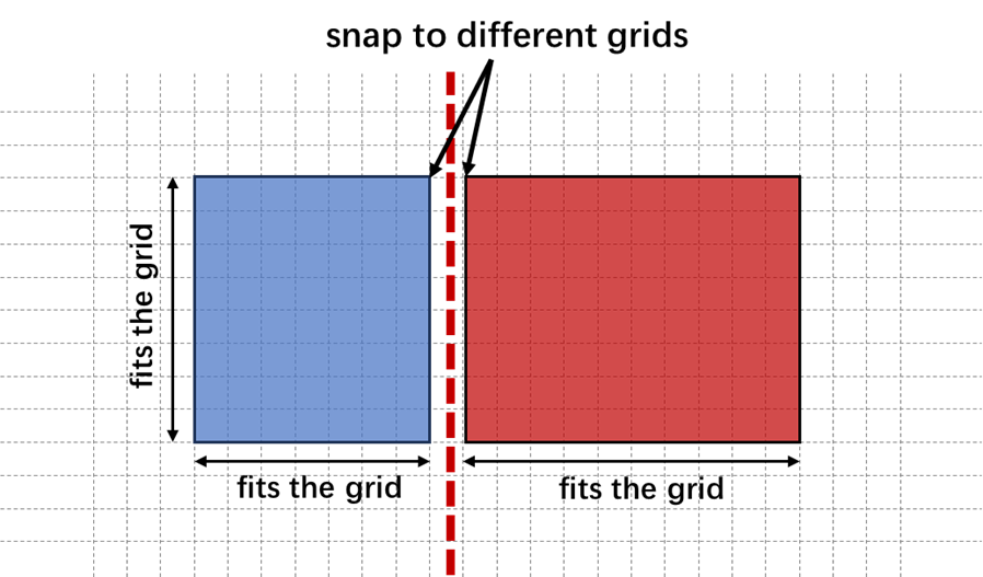
In GDS files, coordinates are internally stored as integer numbers. However, in IPKISS, the coordinates are expressed as floating point numbers. When we export a layout to a GDS file, all IPKISS coordinates are snapped to multiples of the grid unit cell. The points of polygons and the positions of the objects should be both snapped to the grid.
Non-rotated snapping error
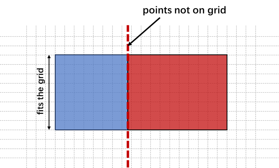
If all the boundary lines of the components are on the grids, there will be no snapping errors, as shown in the figure below.
However, if a boundary line between two components is not perfectly aligned with the grid, the components will be snapped to different grid points in the final GDS file. This results in a grid-distance gap between them, which is a consequence of minor floating-point inaccuracies during the snapping process.
Fixing the snapping error
To fix this DRC violation, we can flatten the layout by creating a flat copy. Flattening a cell means that all the sub-cells of a cell are merged into one cell such that all the elements of the sub-cells are now elements of the cell itself. Flattening removes the hierarchy, ensuring that all resulting transformed coordinates are subject to a single, final snapping event onto the GDSII grid. The following code shows how to do this in IPKISS.
# Fix snapping error
flattened_circuit_lv = i3.LayoutCell(name="flattened_layout").Layout(elements=stubbed_layout.layout.flat_copy())
flattened_circuit_lv.visualize()
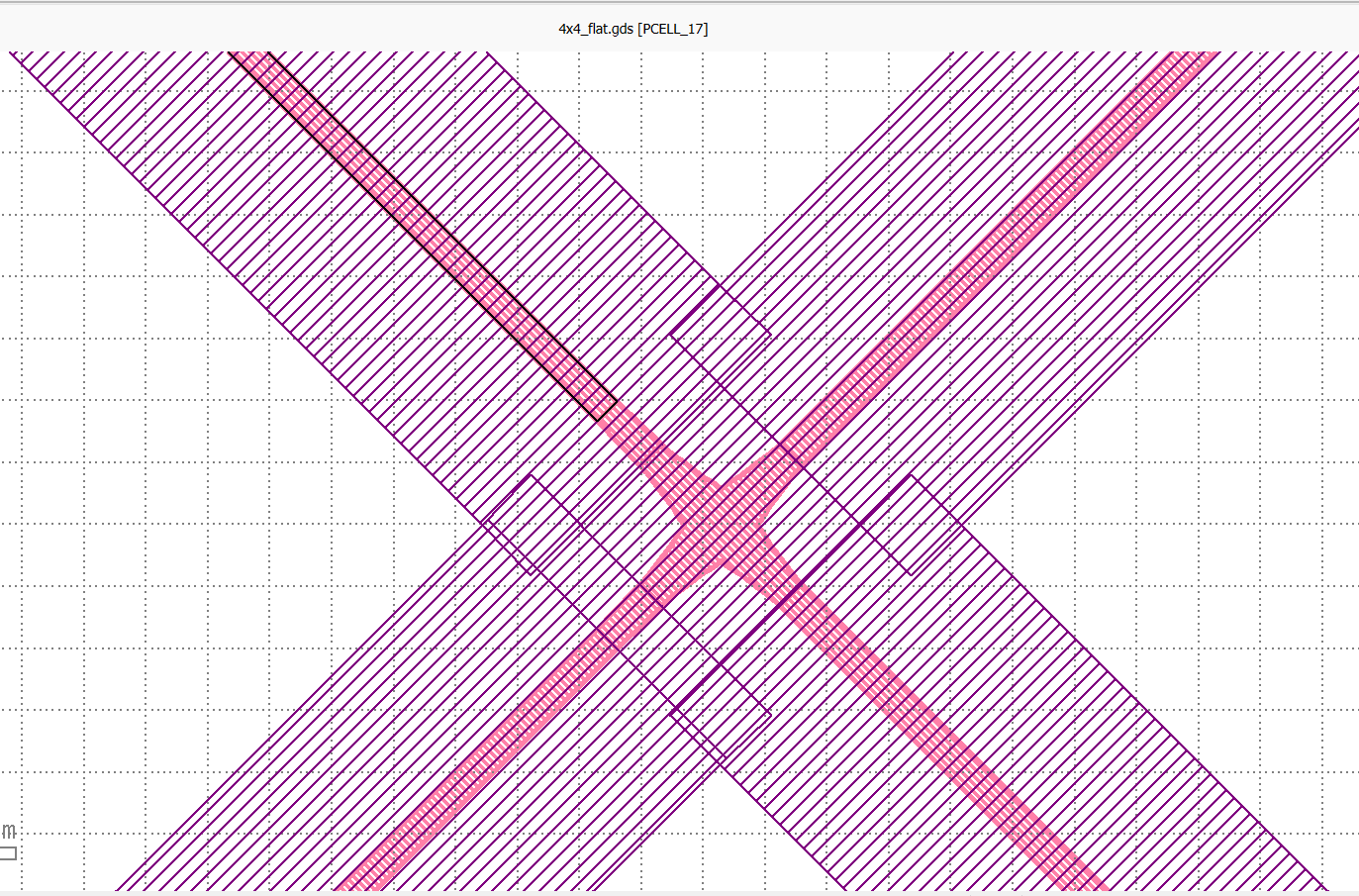
flattened_circuit_lv.write_gdsii("4x4_flat.gds")
Inspecting the GDS in KLayout shows no snapping errors.
Summary
This tutorial taught us how to use IPKISS to find and fix common DRC errors. By automating this process, the software helps designers get their chip ready for tape-out much more quickly.