Define a Directional Coupler PCell for Simulation
Before simulating a component, we first need to create its layout. The dir_coupler folder in the SiFab PDK contains a pcell folder where we store the different PCell variations: /pdks_sources/si_fab/si_fab/ipkiss/si_fab/components/dir_coupler/pcell/cell.py.
What do we mean by variations in this context? To begin, we create a base class for a generic directional coupler. This base class is defined parametrically, allowing for flexibility in the layout by adjusting key design parameters. From this foundation, we can derive additional classes (variations of the base class) tailored to specific applications. For instance, in this tutorial, our primary focus is on creating a specialized PCell where the straight length of the coupler can be varied, while locking all other parameters. Locking parameters that shouldn’t be changed serves as a validation step: if a user tries to instantiate a directional coupler with parameter we don’t have data for, the software can prevent incorrect configurations. As we progress, we will explore how to implement new classes that inherit useful properties from existing ones, making the design process both modular and scalable. These class variations are contained in the same file in the PCell folder.
Define a Base Class PCell
The first step is to create a base class generic directional coupler.
We define a Python class derived from i3.PCell and we call it DirectionalCoupler.
This is done inside the file cell.py.
Inside the DirectionalCoupler class we define a sub-class, class Layout, derived from i3.LayoutView.
This class will contain all the geometric information of the directional coupler.
# Basic directional coupler PCell


class DirectionalCoupler(i3.PCell):
    """
    Directional coupler with customisable layout. Custom functions can be passed as routing_method. This function
    is used to draw the bent section of the directional coupler and takes three parameters as input: bend_length,
    bend_height and adiabatic_angle.
    """

    _name_prefix = "DC"
    trace_template = i3.TraceTemplateProperty(doc="The trace template of the directional coupler")
    routing_method = i3.CallableProperty(
        doc="Routing method for the bends of the directional coupler: ShapeDCSBend or ShapeDCBend"
    )
    straight_length = i3.NonNegativeNumberProperty(default=0.0, doc="Length of the straight section")
    spacing = i3.PositiveNumberProperty(default=0.2, doc="Separation of the straight section sidewall-to-sidewall")
    bend_length = i3.PositiveNumberProperty(default=6.0, doc="Width of the bend section")
    bend_height = i3.PositiveNumberProperty(doc="Height of the bend section")
    adiabatic_angle = i3.PositiveNumberProperty(
        default=5.0, doc="Adiabatic angle for the rounding algorithms of the bends"
    )

    def _default_trace_template(self):
        return SiWireWaveguideTemplate()

    def _default_routing_method(self):
        return ShapeDCBend

    def _default_bend_height(self):
        return self.bend_length

    class Layout(i3.LayoutView):
        @i3.cache()
        def _get_wg_shapes(self):
            """This method returns the shape of the top and bottom arms of the directional coupler."""
            core_width = self.trace_template.core_width
            y1 = self.spacing / 2.0 + core_width / 2.0
            x1 = self.straight_length / 2.0

            # Calculation of top-right shape
            straight_middle = i3.Shape([(0.0, y1), (x1, y1)])
            bend = self.routing_method(
                bend_length=self.bend_length, bend_height=self.bend_height, adiabatic_angle=self.adiabatic_angle
            )
            bend_transformed = bend.transform_copy(transformation=i3.Translation((x1, y1)))
            top_right_shape = straight_middle + bend_transformed

            # Calculation of top and bottom shapes
            top_shape = top_right_shape.transform_copy(transformation=i3.HMirror()).reversed() + top_right_shape
            bottom_shape = top_shape.transform_copy(transformation=i3.VMirror())
            top_shape.start_face_angle, top_shape.end_face_angle = top_shape.get_face_angles()
            bottom_shape.start_face_angle, bottom_shape.end_face_angle = bottom_shape.get_face_angles()
            top_shape[0] = i3.snap_coordinate(top_shape[0])
            top_shape[-1] = i3.snap_coordinate(top_shape[-1])
            bottom_shape[0] = i3.snap_coordinate(bottom_shape[0])
            bottom_shape[-1] = i3.snap_coordinate(bottom_shape[-1])

            return top_shape, bottom_shape

        def generate(self, layout):
            trace_template = self.trace_template
            cladding_layer = trace_template.cladding_layer
            top, bottom = self._get_wg_shapes()  # wg0 = top, wg1 = bottom
            # we use the trace template to generate the elements for the shapes of both waveguides
            # as IPKISS carefully controls the core and cladding layer drawing
            wg0 = trace_template(shape=top)
            wg1 = trace_template(shape=bottom)
            # merge the cladding layers into one and avoid acute angles, leaving the core layer unchanged
            layout += i3.stub_acute_angles(wg0.elements + wg1.elements, layers=[cladding_layer])

            # Ports
            layout += i3.OpticalPort(
                position=bottom.points[0],
                name="in1",
                angle=bottom.start_face_angle + 180.0,
                trace_template=trace_template,
            )
            layout += i3.OpticalPort(
                position=top.points[0],
                name="in2",
                angle=top.start_face_angle + 180.0,
                trace_template=trace_template,
            )
            layout += i3.OpticalPort(
                position=bottom.points[-1],
                name="out1",
                angle=bottom.end_face_angle,
                trace_template=trace_template,
            )
            layout += i3.OpticalPort(
                position=top.points[-1],
                name="out2",
                angle=top.end_face_angle,
                trace_template=trace_template,
            )
            return layout
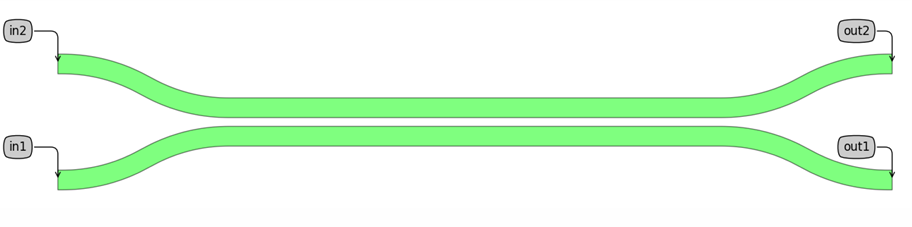
Inspecting the layout shows
Let’s analyze the code above:
Properties. We define a list of properties that will be used to design the directional coupler. The order of these properties can be altered. Each property has a default value: if the user does not supply a value, this default will be used.
Layout class. We define the Layout class inside the
DirectionalCouplerPCell. This class is a Layout View.The
_get_wg_shapesmethod generates the shapes of the top and bottom arms of a directional coupler. The design approach is to first define the shape of the top-right arm of the directional coupler. This is done by first drawing a straight segment from (0, y1) to (x1, y1). A bend section is then generated using self.routing_method, which defines how the waveguide curves. The bend is then translated to connect smoothly with the straight segment. The final top-right shape is the combination of the straight segment and the transformed bend. The full top waveguide is created by mirroring the top-right section horizontally and joining it with itself. The bottom waveguide is obtained by vertically mirroring the top waveguide. We then snap the coordinates to the grid to avoid drc errors.Inside the method
generate(self, layout), we first define the geometrical elements of the directional coupler:trace_template: We make a parametertrace_templatethat takes the value of thetrace_templatedefined in the PCell properties at the top of the class. For more details about trace templates, please refer to this tutorial Connectors, trace templates and waveguides.cladding_layer: Parameter that retrieves the cladding layer from the trace template.wg0_shape,wg1_shape: Parameters that take the results of the shape calculation done in the_get_wg_shapesmethodwg0andwg1: Draw the specified trace template along the shape that was defined in_get_wg_shapesfor the top and bottom waveguides respectively.i3.stub_acute_angles(wg0.elements + wg1.elements, layers=[cladding_layer])is used to add stubs to the directional coupler to avoid sharp angles which would raise DRC errors.
Inside the same
generate(self, layout)method, we add 4 ports: in1, in2, out1 and out2. Each port is created usingi3.OpticalPortand needs the following properties to be set:name: name of the port.position: position of the port.angle: direction in which a waveguide leaving the port has to go. 0 degrees is parallel to the x-axis, going eastwards.trace_template: it denotes the trace template of waveguide used at the port.
In a directional coupler, the ports are not simply horizontal or vertical. Instead, their angles depend on the shape of the waveguides.
Each waveguide shape (top and bottom) has an associated start and end face angle. The input ports (in1, in2) are assigned an angle of
start_face_angle+ 180.0 to correctly orient them opposite to the waveguide’s direction. The output ports (out1, out2) directlyend_face_angle, ensuring continuity with the waveguide path.
Simulation Recipe for the Directional Coupler
We define a simulation recipe that uses Ansys Lumerical FDTD via the Luceda Link for Ansys Lumerical.
This simulation recipe is added to the simulation subfolder, in a file called simulate_lumerical.py.
For a detailed look at how to create a simulation script, please refer to the following tutorial: Ansys Lumerical FDTD.
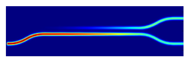
Now that a simulation recipe is defined, it can be executed from IPKISS and the simulation job is exported to the Ansys Lumerical FDTD solver. The FDTD solver will calculate how the electromagnetic field propagates through the directional coupler. The result of this simulation can be seen here with the power being split 50:50 in each waveguide.
Once we have run the simulation and retrieved the results, we can use this data to build a compact model for the directional coupler which will be used to create a circuit model.
Defining a Circuit Model for a (Locked) Directional Coupler
Now that we have implemented a simulation recipe, we will define a circuit model for a directional coupler that can use the results of this simulation.
The first step is to implement a compact model which describes the behavior of the component. This is done in compactmodels/dir_coupler.py. However, before building your own model, first check the Compact model library to see if one already fits your needs. If not, IPKISS allows you to define your own custom linear or nonlinear models. If you’re unfamiliar with compact models, have a look at this tutorial: Compact models
The second step is to define a fixed directional coupler PCell that uses the compact model in components/dir_coupler/pcell/cell.py.
The third step is to define a regeneration script that can run the simulation recipe on the fixed PCell and return the data required by the compact model of the fixed cell components/dir_coupler/regeneration/regenerate_si_directional.py.
Step 1: Implementing a Compact Model
In our folder structure, we keep models separate from components in a folder called compactmodels.
Remember you can always consult the Compact model library
for existing models or inspiration.
Let’s now take a look at the implementation of a custom compact model for the directional coupler below:
class DCCompactModel(CompactModel):
    """Directional coupler compact model based on kappa0 and kappa (kappa0: coupling at zero length).
    The model has a constant phase difference of pi/2 between the cross and throguh ports, which is only
    accurate for lossless symmetrical directional couplers.
    The input parameters are the center_wavelength and the coefficients of the polynomial fit of kappa0, kappa,
    length, transmission and reflection as a function of wavelength.
    """

    parameters = [
        "center_wavelength",
        "kappa0",
        "kappa",
        "length",
        "transmission",
        "reflection",
    ]

    terms = [
        OpticalTerm(name="in1"),
        OpticalTerm(name="in2"),
        OpticalTerm(name="out1"),
        OpticalTerm(name="out2"),
    ]

    def calculate_smatrix(parameters, env, S):
        kappa = np.polyval(parameters.kappa, env.wavelength - parameters.center_wavelength)
        kappa0 = np.polyval(parameters.kappa0, env.wavelength - parameters.center_wavelength)
        transmission = np.sqrt(np.polyval(parameters.transmission, env.wavelength - parameters.center_wavelength))
        reflection = np.sqrt(np.polyval(parameters.reflection, env.wavelength - parameters.center_wavelength))
        coupling = 1j * transmission * np.sin(kappa0 + parameters.length * kappa)
        tru = transmission * np.cos(kappa0 + parameters.length * kappa)
        S["in1", "out1"] = S["out1", "in1"] = S["in2", "out2"] = S["out2", "in2"] = tru
        S["in2", "out1"] = S["out1", "in2"] = S["in1", "out2"] = S["out2", "in1"] = coupling
        S["in1", "in1"] = S["out1", "out1"] = S["in2", "in2"] = S["out2", "out2"] = reflection
Our compact model inherits from the class CompactModel in Luceda IPKISS.
This code defines key parameters, optical ports, and a method to compute the S-matrix, which describes how light propagates through the device.
First, it establishes the model parameters, including the center wavelength, coupling coefficients (kappa, kappa0), length, transmission, and reflection.
These parameters define how light is split, transmitted, or reflected based on wavelength.
The four optical ports - in1, in2, out1, and out2 - represent the directional coupler interfaces where light enters and exits.
The calculate_smatrix function describes how optical power is transferred between ports based on wavelength-dependent polynomial evaluations of coupling, transmission, and reflection.
Using trigonometric functions, the function calculates the power transfer (coupling) between waveguides and the through transmission, ensuring accurate modeling of signal propagation.
The model has a constant phase difference of π/2 between the cross and through ports, which is only accurate for lossless symmetrical directional couplers.
Step 2: Define a New Locked PCell for an S-Shaped Silicon Directional Coupler That Uses the Compact Model
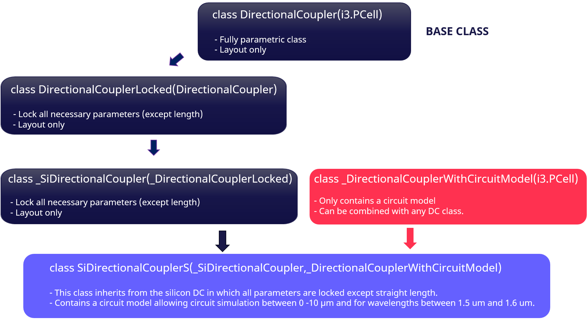
Now, we are ready to use the compact model in the circuit model view of the directional coupler PCell. The goal is to create a new PCell for a silicon S-shaped directional coupler that has a circuit model. As we will see, an ideal structure for the pcell folder is to have multiple variations of the component by inheriting from more general PCells. By defining multiple versions of a PCell, you can quickly iterate and explore different design options. This is particularly useful when you want to test variations of a component, such as different geometries or material properties, without creating entirely new files or classes for each variation. Let’s look at how we can do that.
First, we create a directional coupler where all the properties aside from the straight length are locked.
This involves creating a new class _DirectionalCouplerLocked that inherits from DirectionalCoupler, which was defined at the beginning.
class _DirectionalCouplerLocked(DirectionalCoupler):
    """Abstract class for directional coupler where all the properties aside from the length (straight_length) are
    locked."""

    trace_template = i3.LockedProperty()
    data_tag = i3.LockedProperty()
    routing_method = i3.LockedProperty()
    spacing = i3.LockedProperty()
    bend_length = i3.LockedProperty()
    bend_height = i3.LockedProperty()
    adiabatic_angle = i3.LockedProperty()

    def _default_name(self):
        length_nano_meters = int(self.straight_length * 1000.0)
        return self.data_tag.upper() + f"_{length_nano_meters}"
Using this we create a silicon directional coupler in which all parameters are optimized except for the length.
class _SiDirectionalCoupler(_DirectionalCouplerLocked):
    """Abstract class for a silicon wire directional couplers where all the properties aside from the length
    (straight_length) are optimized and locked."""

    def _default_trace_template(self):
        return SiWireWaveguideTemplate(name=self.name + "_si_trace_template")

    def _default_spacing(self):
        return 0.2

    def _default_adiabatic_angle(self):
        return 1.0
Next, we create an abstract class for a directional coupler with a circuit model that calculates the coupling from the fitted polynomials for the coupling coefficient.
class _DirectionalCouplerWithCircuitModel(i3.PCell):
    """Abstract class for a directional coupler with a circuit model that calculate the coupling from the fitted
    polynomials for the coupling coefficient.
    """

    class CircuitModel(i3.CircuitModelView):
        def _generate_model(self):
            center_wavelength, pol_transmission, pol_kappa0, pol_kappa = get_data(data_tag=self.data_tag)
            return DCCompactModel(
                center_wavelength=center_wavelength,
                transmission=pol_transmission,
                kappa0=pol_kappa0,
                kappa=pol_kappa,
                length=self.cell.straight_length,
                reflection=np.array([0.0]),
            )
As we can see, structuring the pcell folder this way allows for multiple variations of a given component whereby we create a new class that inherits from a more general class.
To continue this tutorial, we will create a new class called SiDirectionalCouplerS which is an S-shaped directional coupler.
This class inherits from:
_SiDirectionalCouplerto define a layout based on an SOI stack where all parameters but the length are optimized and locked._DirectionalCouplerWithCircuitModelto add the circuit model to the silicon directional coupler layout.
class SiDirectionalCouplerS(_SiDirectionalCoupler, _DirectionalCouplerWithCircuitModel):
    """
    Silicon wire directional coupler with a S-shape, where all the properties aside from the length (straight_length)
    are optimized and locked.
    Circuit simulation data is available for any length and for wavelengths between 1.5 um and 1.6 um.

    Note that the compact model is based on artificial simulation results as the technology
    and components are fictional. The model only serves demonstration purposes.
    """

    def _default_data_tag(self):
        return "si_directional_coupler_s"

    def _default_routing_method(self):
        return ShapeDCSBend

    def _default_bend_length(self):
        return 4.0

    def _default_bend_height(self):
        return 1.0

    class CircuitModel(_DirectionalCouplerWithCircuitModel.CircuitModel):
        pass
Schematic View of the Class Structure
Let’s summarize the classes we have implemented. We can view the class structure found in components/dir_coupler/pcell/cell.py in the following schematic.
Conclusion
We began by designing a base class for a parametric directional coupler PCell, providing a flexible template for layout definition. Next, we created a locked class, where all parameters were fixed except for the straight length, ensuring controlled variation. Building on this, we introduced a technology-specific class, defining the coupler for silicon integration. Additionally, we developed a circuit model class, designed to be attachable to any directional coupler variant. Finally, we combined these elements into a new silicon directional coupler class, inheriting the locked properties and circuit model, resulting in a fully defined, reusable component.