Waveguides
We have seen that a connector generates a combination of waveguides and tapers to create a connection between ports. It is also possible to create an individual waveguide or taper in IPKISS. They can be used to create the layout of a component (see step 2 of Creating a Hierarchical Layout) or can also be inserted as connections between ports within a circuit. The latter is useful when you want to create a connection that follows a customized shape that cannot be created using a connector.
In IPKISS, waveguides and tapers are not just drawings, but they are fully parametric cells (PCells) that work and behave like any other PCell. This provides a number of benefits:
They are parametrized, allowing you to control their parameters (e.g., shape, bend radius, …) directly within IPKISS.
They can be modeled by running physical simulations (e.g. mode propagation tools or FDTD) and included in circuit simulations just like other PCells.
In this section about waveguides, we will first see how to instantiate a rounded waveguide and visualize it. After that, we will create and visualize a waveguide with a more complex, specific shape. Finally, we will briefly discuss waveguide transitions.
Rounded waveguide
A waveguide is created by drawing a trace template over a specified shape.
The i3.RoundedWaveguide class creates a waveguide with a rounded shape, determined by the specified rounding parameters.
Let’s have a look at the code below that creates and visualizes this type of waveguide.
from si_fab import all as pdk
from ipkiss3 import all as i3

# Define trace template of the wire waveguide
wg_t = pdk.SiWireWaveguideTemplate()
wg_t.Layout(core_width=1.0, cladding_width=2 * 3.0 + 1.0)

# Define shape of the trace
shape = [(0.0, 0.0), (10.0, 0), (10.0, 10.0), (20.0, 20.0), (30.0, 0.0), (40.0, 40.0)]
i3.Shape(shape).visualize()

# Instantiating the waveguide: we use the RoundedWaveguide class and specify the trace template
wg = i3.RoundedWaveguide(trace_template=wg_t)
wg_l = wg.Layout(
    shape=shape,
    bend_radius=5.0,
)
wg_l.visualize()
wg_l.cross_section(cross_section_path=i3.Shape([(2.0, -5.0), (2.0, 5.0)])).visualize()
wg_l.write_gdsii("test.gds")
First, the trace template of a wire waveguide out of the si_fab PDK is instantiated. Afterwards, the shape of the waveguide is defined and visualized. In this case, the shape is a combination of discrete lines that will be transformed into a rounded shape using a desired rounding algorithm.
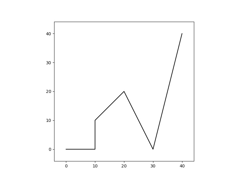
Shape of discrete lines
Next, the waveguide is created by specifying the trace template. The following step is to pass the shape of the waveguide to the Layout view of the waveguide. The waveguide can now be visualized.
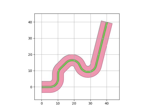
Layout of the rounded waveguide
The virtual fabrication of a waveguide is dependent on the trace template and the layers defined in the technology of the PDK. A cross-section through a specified path is also virtually fabricated and visualized in this code example. Eventually, the GDS file with the layout is also exported.
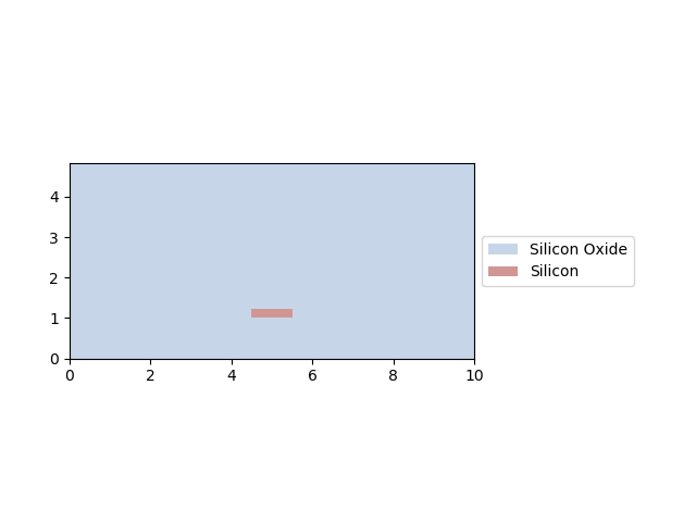
Virtual fabrication of cross-section through the cross-section path
Waveguide with a specific shape
When designing a component (such as a directional coupler), it might be required to create waveguides with a very specific shape. Alternatively, when connecting your ports, you may need to create a waveguide connection with a customized shape that cannot be created by a connector. In the IPKISS API reference, you can find a list of specific shapes that can be used for such purposes: Geometry Reference.
The code below creates a rib waveguide along a Hermite S-bend shape and visualizes the shape, the waveguide layout and the cross-section along the cross-section path. Additionally, the cross-section path is visualized together with the waveguide.
from si_fab import all as pdk
from ipkiss3 import all as i3
import matplotlib.pyplot as plt

# Define trace template of the rib waveguide
wg_t = pdk.SiRibWaveguideTemplate()
wg_t.Layout(core_width=1.0, cladding_width=2.0)

# Define trace
shape = i3.ShapeHermiteSBend(x_offset=30.0, y_offset=-20.0, start_point=(0, 0))
i3.Shape(shape).visualize()

# Instantiating the waveguide with Hermite S-bend shape
wg = i3.RoundedWaveguide(trace_template=wg_t)
wg_l = wg.Layout(
    shape=shape,
    bend_radius=0.1,
)
fig = plt.figure()
wg_l.visualize(figure=fig, show=False)
ax = fig.gca()
ax.plot((2, 2), (2, -2), color="black", linewidth=1.0, linestyle="--")  # Adding cross-section path to plot
plt.show()

wg_l.cross_section(cross_section_path=i3.Shape([(2.0, -2.0), (2.0, 2.0)])).visualize()
wg_l.write_gdsii("test.gds")
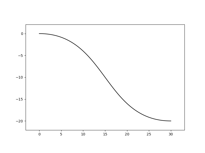
Visualization of Hermite S-bend shape
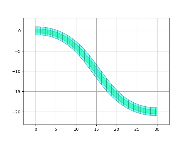
Layout of the waveguide and cross-section path through the waveguide (dotted line)
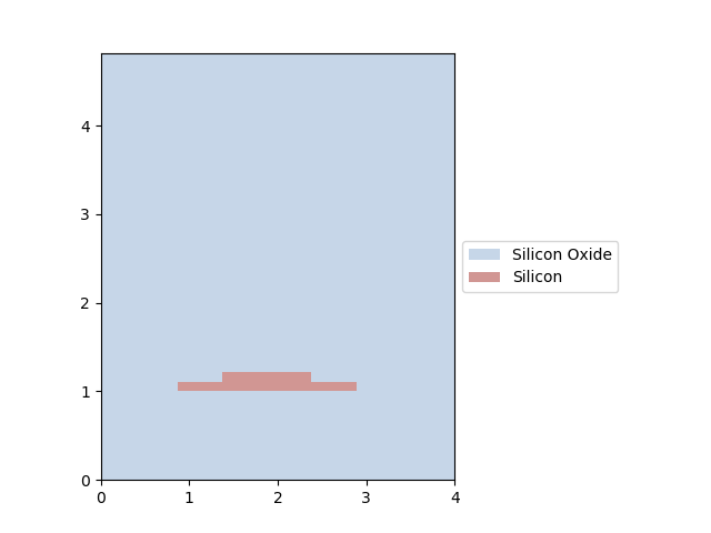
Virtual fabrication of cross-section through the cross-section path
Waveguide transitions
In photonic circuit design the term waveguide transition and taper are often used as synonyms. As explained in the section about trace templates, if you use connectors to connect different components together, tapers will be generated automatically between ports with different trace templates. Which tapers are generated by these connectors are defined in the used PDK. If you need a specific taper that a connector is not yet able to generate, you can define a custom waveguide transition and insert this as a connection inside your circuit.
You can define such a waveguide transition with i3.LinearWindowWaveguideTransition.
This creates a waveguide transition that tapers linearly from one trace template to another.
Other types of transitions, such as parabolic or exponential, can be found in Transitions.