MMI Optimization and Model Attachment for Circuit Simulation
Note
This tutorial requires an installation of the Luceda Link for Tidy3D. Please contact us for a trial license. For more detail on how to perform physical device simulation in Luceda IPKISS, please follow the Physical Device Simulation Flow tutorial, in particular the section on Tidy3D tutorial.
Introduction
When designing a photonic integrated circuit, it is often important to perform device-level simulations to optimize the layout parameters of components for a given application. This may be the case when designing new components from scratch or when dealing with parametric cells from a Process Design Kit (PDK), which may only provide layout information without a corresponding simulation model that describes the component behavior in a circuit. Adding a circuit model to the component allows for circuit-level simulations, enabling a more thorough analysis of the performance of these circuits when they contain these components.
This tutorial shows how to optimize a 1x2 Multi-Mode Interferometer (MMI) from the SiFab PDK for operation at a wavelength of 1550 nm, using an automated optimization routine that launches simulations in Tidy3D from the IPKISS environment via Luceda Link for Tidy3D. Once the device-level optimization is achieved, the next step involves building a compact model for this component using the data obtained from the physical device simulation. This model is essential for using the MMI in a parametric splitter tree circuit and for analyzing the circuit performance by running circuit-level simulations with IPKISS Caphe.
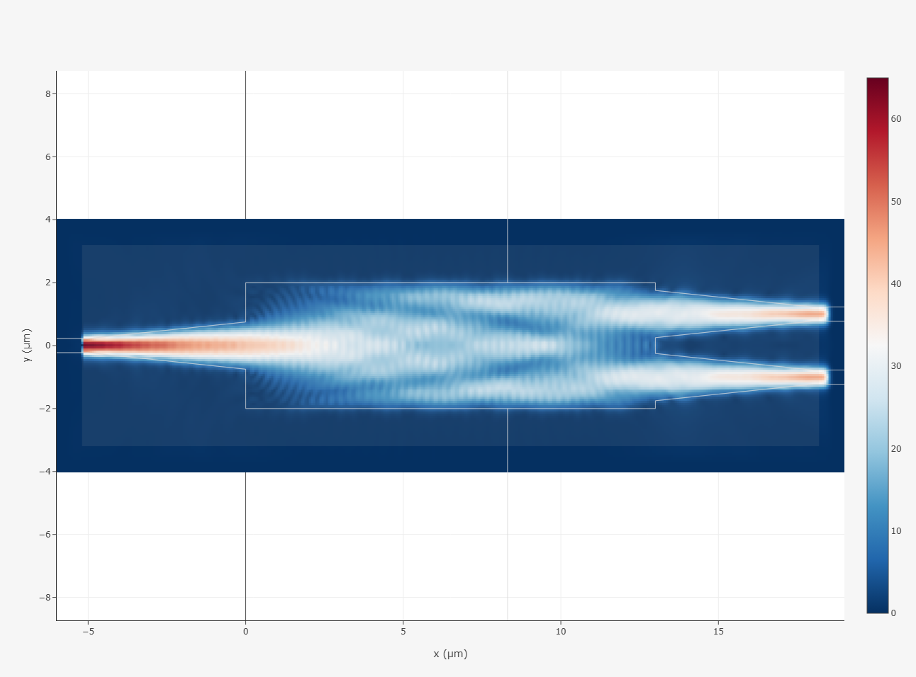
Visualizing field propagation in the optimized MMI using Luceda link for Tidy3D.
The process includes the following steps:
Defining a simulation recipe that uses Luceda Link for Tidy3D to automatically run physical device simulations on an IPKISS layout, using Tidy3D in the cloud.
Sweeping layout parameters and plotting the resulting data.
Defining a new PCell with locked layout parameters obtained from the optimization results.
Adding the circuit model to the PCell that can be used in circuit simulations.
Designing and simulating a splitter tree using the the optimized PCell.
Defining a simulation recipe
First, we need to define a simulation recipe that will use the Luceda Link for Tidy3D to launch a simulation using Tidy3D’s FDTD engine. For this purpose, we define a function called simulate_mmi_by_tidy3d that takes the MMI layout, a wavelength range, and a central wavelength as inputs. The function then returns the simulation results and stores them both locally and on Tidy3D’s cloud which is accessible through a web GUI. For more details about setting up different parameters for a simulation job using Luceda Link for Tidy3D please look at this Tidy3D tutorial.
def simulate_mmi_by_tidy3d(mmi_layout, wavelength_range, central_wavelength, sim_name=""):
    """Performs an FDTD simulation of a given MMI layout.
     The obtained s-matrix is returned and saved to a file.

     Parameters
     ----------
     mmi_layout : LayoutView
        Layout view of the MMI
     wavelength_range : tuple[float, float, int]
        The range of wavelengths for the simulation in the format (start_wavelength, end_wavelength, num_wavelengths)
     central_wavelength : float
        The center wavelength for the simulation
     sim_name : str, optional
        An optional suffix for the output Touchstone file containing the obtained s-matrix

    Returns
    -------
    The resulting s-matrix of the simulated component
    """
    sim_geom = i3.device_sim.SimulationGeometry(layout=mmi_layout)
    task_folder_name = "mmi_optimization"
    task_name = "mmi"
    name = "smatrix" + sim_name

    base_directory = os.path.join(os.path.dirname(os.path.realpath(__file__)), "..", "data")

    simulation = i3.device_sim.Tidy3DFDTDSimulation(
        geometry=sim_geom,
        task_name=task_name,
        task_folder_name=task_folder_name,
        project_folder=os.path.join(base_directory, "mmi_1x2_optimized_1550_fdtd"),
        monitors=[
            i3.device_sim.Port(name="in1", box_size=(2.0, 1.0)),
            i3.device_sim.Port(name="out1", box_size=(2.0, 1.0)),
            i3.device_sim.Port(name="out2", box_size=(2.0, 1.0)),
        ],
        outputs=[i3.device_sim.SMatrixOutput(name=name, wavelength_range=wavelength_range)],
        solver_material_map={i3.TECH.MATERIALS.SILICON: "cSi - Palik_Lossless"},
        setup_macros=[
            i3.device_sim.tidy3d_macros.fdtd_auto_grid_spec(min_steps_per_wavelength=15),
            i3.device_sim.tidy3d_macros.fdtd_run_time(run_time=1.5e-12),
        ],
        center_wavelength=central_wavelength,
    )

    return simulation.get_result(name=name)
Sweeping over layout parameters and plotting data
Once the simulation recipe is defined, the next step involves sweeping over a layout parameter, in this case, the length of the MMI. By varying this parameter, we can identify the optimal length that provides the best transmission at 1550 nm. The following code defines a range of MMI lengths to sweep over, creating an instance of the MMI component for each length. The previously defined simulate_mmi_by_tidy3d function simulates each MMI instance. After the simulations, transmission and reflection data for each length are extracted and stored in the si_fab/components/mmi/data/mmi_1x2_optimized_1550_fdtd folder. Finally, the results of transmission and back-reflection at the ports are plotted for each length. The plot in Figure 1 shows that the maximum transmission occurs at the length of 13 µm.
mmi_lengths = np.linspace(10.0, 16.0, 13)
central_wavelength = 1.55
wavelength_range = (1.5, 1.6, 11)

transmission_out = []
reflection_in = []
reflection_out = []

for length in mmi_lengths:
    print(f"Length = {length} µm")

    mmi = pdk.MMI1x2(
        trace_template=pdk.SiWireWaveguideTemplate(),
        width=4.0,
        length=length,
        taper_width=1.5,
        taper_length=5,
        waveguide_spacing=2.01,
        cladding_width=8.0,
    )
    MMI_lo = mmi.get_default_view(i3.LayoutView)

    smatrix = simulate_mmi_by_tidy3d(MMI_lo, wavelength_range, central_wavelength, sim_name=str(length))

    idx = np.argmin(np.abs(central_wavelength - smatrix.sweep_parameter_values))
    transmission_out.append(np.abs(smatrix["out1", "in1", idx]) ** 2)
    reflection_in.append(np.abs(smatrix["in1", "in1", idx]) ** 2)
    reflection_out.append(np.abs(smatrix["out1", "out1", idx]) ** 2)

plt.figure()
plt.plot(mmi_lengths, transmission_out, "C0-", marker="o", label="in1 > out1")
plt.plot(mmi_lengths, reflection_in, "C1-", marker="o", label="in1 > in1")
plt.plot(mmi_lengths, reflection_out, "C2-", marker="o", label="out1 > out1")
plt.xlabel("MMI length (µm)")
plt.ylabel("Transmission")
plt.legend()
plt.show()
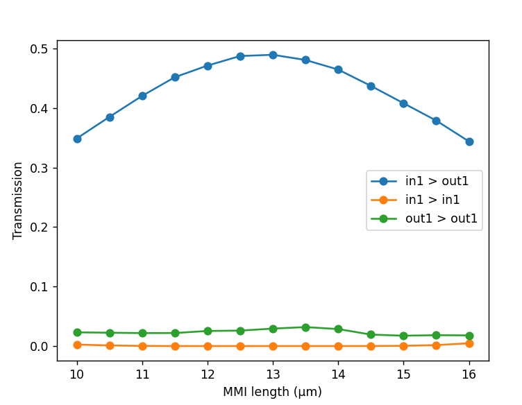
Figure 1. Transmission and reflection at the MMI ports for different lengths.
Defining a new PCell
After determining the optimal MMI length, the next step is to create a new PCell with these optimized parameters. We add MMI1x2Optimized1550FDTD to the SiFab demo PDK. Below is the code to define a new PCell for the MMI component, optimized for maximum transmission at 1550 nm:
class MMI1x2Optimized1550FDTD(MMI1x2):
    """MMI1x2 with layout parameters optimized for maximum transmission at 1550 nm.
    CircuitModel interpolated from s-matrix obtained with a Tidy3D FDTD simulation.

    Note that the compact model is based on artificial simulation results as the technology
    and components are fictional. The model only serves demonstration purposes.
    """

    data_tag = i3.LockedProperty()

    def _default_data_tag(self):
        return "mmi_1x2_optimized_1550_fdtd"

    def _default_name(self):
        return self.data_tag.upper()

    def _default_trace_template(self):
        tt = SiWireWaveguideTemplate(name=self.name + "_tmpl")
        tt.Layout(core_width=0.45)
        return tt

    def _default_width(self):
        return 4.0

    def _default_length(self):
        return 13

    def _default_taper_width(self):
        return 1.5

    def _default_taper_length(self):
        return 5.0

    def _default_waveguide_spacing(self):
        return i3.snap_value(2.00359857317 / 2.0) * 2.0  # Snap to twice the grid size so that the edges are on the grid
The new MMI1x2Optimized1550FDTD PCell inherits from the generic MMI1x2 class, which is a fully parametric, non-optimized MMI. By inheriting from this MMI, we avoid the need to redefine the MMI layout and can simply overwrite the default parameter values with the optimized layout parameters obtained from the simulation.
Implementing the circuit model
With the optimized MMI PCell defined, the next step is to implement the circuit model that uses the FDTD simulation data. In MMI1x2Optimized1550FDTD, the CircuitModel subclass generates the circuit model for this component based on S-matrix data. Here we use the S-matrix data obtained from the Tidy3D FDTD simulation for the MMI length of 13 µm to create a spline-based representation of the component’s behavior over a range of wavelengths.
    # Generate a BSplineSModel from an SMatrix1DSweep
    class CircuitModel(i3.CircuitModelView):
        def _generate_model(self):
            smatrix_path = os.path.join(
                os.path.dirname(os.path.realpath(__file__)), os.pardir, "data", self.data_tag, "smatrix13.0.s3p"
            )
            smat = convert_smatrix_units(
                i3.device_sim.SMatrix1DSweep.from_touchstone(smatrix_path),
                to_unit="um",
            )
            bsplinesmodel = i3.circuit_sim.BSplineSModel.from_smatrix(smat, k=3)
            return bsplinesmodel
This circuit model defines the component’s performance within a larger circuit, and facilitates faster simulation of the entire circuit. One can therefore change layout parameters of the circuit, and see how the circuit simulation is affected by these layout parameters. More information about using scatter matrix files for running circuit simulation can be found here.
Splitter tree simulation using the optimized MMI
This section demonstrates how to perform a circuit simulation using the MMI1x2Optimized1550FDTD PCell. We first instantiate a splitter tree and import the MMI1x2Optimized1550FDTD cell from the PDK to be used as the splitter PCell inside the splitter tree circuit. We can also define some other layout parameters, such as the number of levels.
from si_fab import all as pdk
from pteam_library_si_fab import all as lib
import numpy as np

n_levels = 3  # Number of levels of the splitter tree we want to create

# First, we instantiate the unrouted splitter tree. As splitter, we use the MMI in the SiFab demo PDK that
# was optimized using FlexCompute's Tidy3D.

splitter_tree = lib.SplitterTree(
    splitter=pdk.MMI1x2Optimized1550FDTD(),
    levels=n_levels,
    spacing_x=100,
    spacing_y=50,
)
Then, we use this splitter tree to instantiate a routed splitter tree, which takes our initial splitter tree and routes it to optical inputs and outputs (fiber grating couplers).
circuit = lib.RoutedSplitterTree(
    splitter_tree=splitter_tree,
    gc=pdk.FC_TE_1550(),
)
Both the splitter tree and the routed splitter tree are defined in our custom team library based on the SiFab technology (pteam_library_si_fab). This way, these designs can be reused many times without duplicating code. Additionally, they are defined parametrically, offering significant flexibility for parameter adjustments. For example, the default splitter and grating coupler PCells can be easily replaced with their counterparts designed for optimal operation at 1310 nm when instantiating the splitter tree. This eliminates the need to redesign the entire tree.
Figure 2. shows the layout of the routed splitter tree:
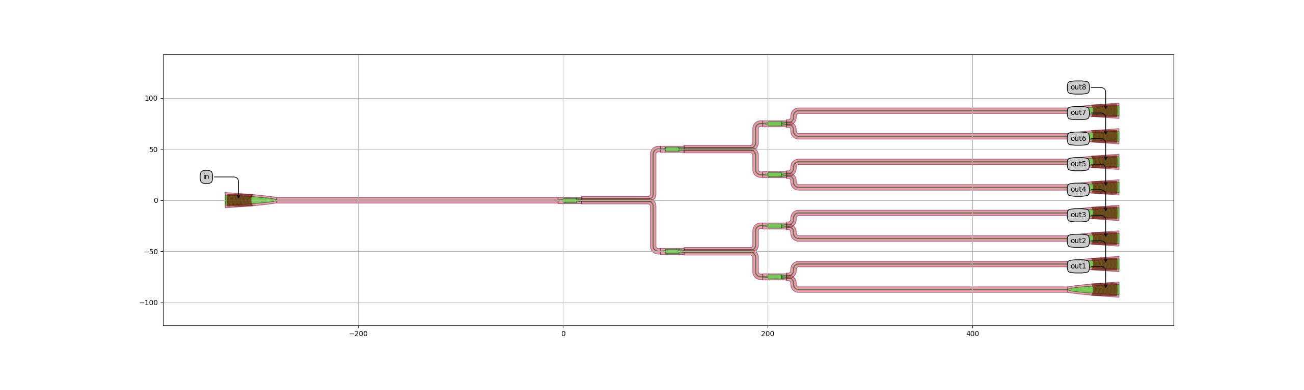
Figure 2. Routed three-level splitter tree.
We now instantiate the CircuitModelView of the circuit and call get_smatrix to run the circuit simulation.
Using the visualize method, we can plot the results of an S-matrix frequency sweep between defined pairs of ports:
circuit_model = circuit.CircuitModel()
wavelengths = np.linspace(1.5, 1.6, 501)
S_total = circuit_model.get_smatrix(wavelengths=wavelengths)

term_pairs = [("in", "in")]
for n in range(n_levels**2 - 1):
    term_pairs.append(("in", f"out{n + 1}"))

S_total.visualize(term_pairs=term_pairs, figsize=(8, 5), scale="dB", yrange=(-80.0, 0.0))
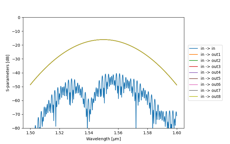
Figure 3. Simulation of the three-level splitter tree in frequency domain.
We can easily observe the effect of adding an additional level to the splitter tree by setting n_levels = 4. The layout of a four-level splitter tree is shown in Figure 4. Comparing the circuit simulation results in Figure 5 with those for n_levels = 3 plotted in Figure 3, we notice a 3 dB drop in transmission to the output ports.
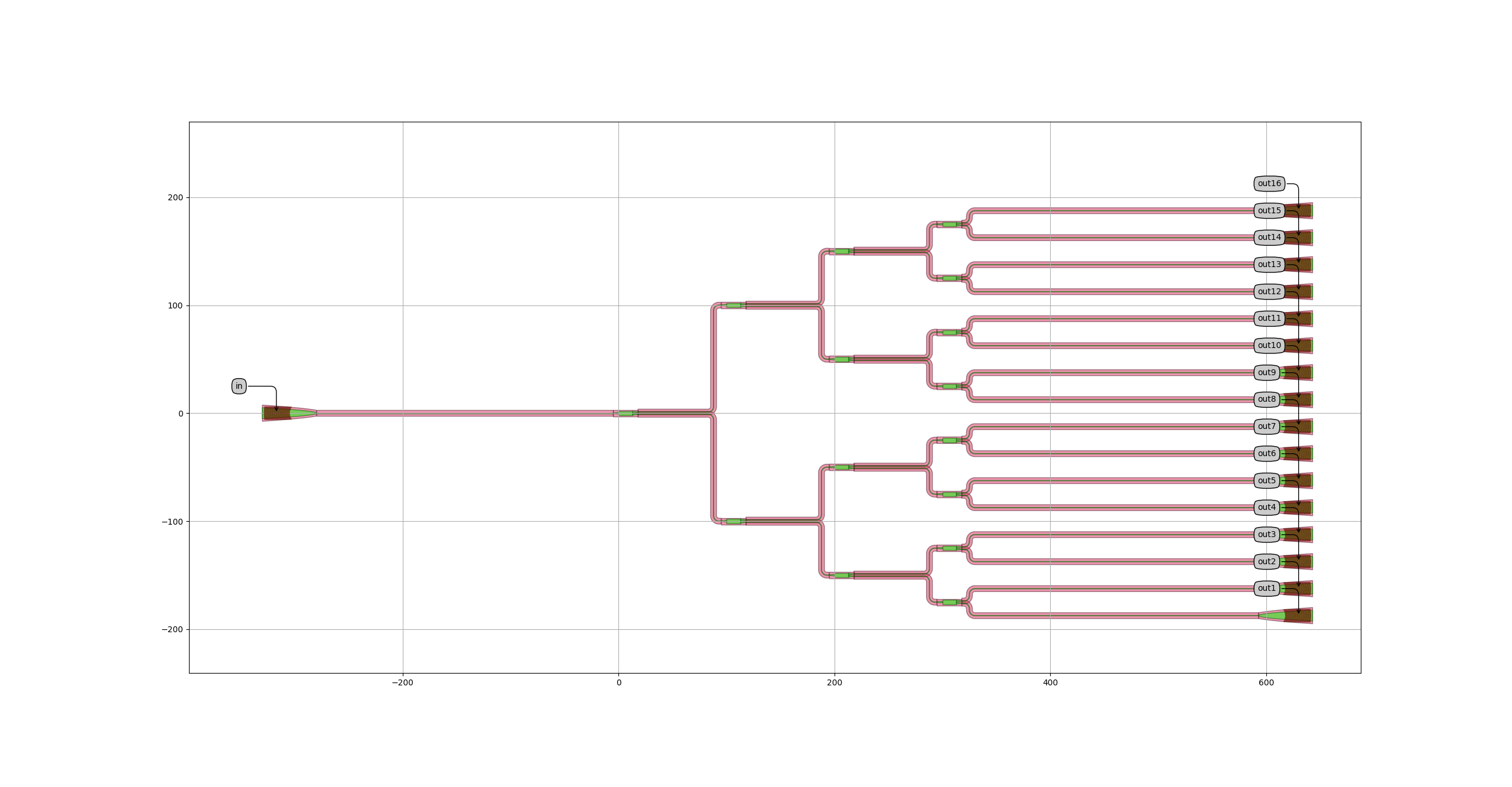
Figure 4. Routed four-level splitter tree.
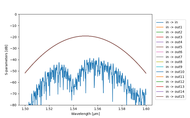
Figure 5. Simulation of the four-level splitter tree in frequency domain.
Note
The above simulation results are artificial results as they’re based on fictional technology and components. These only serve demonstration purposes.