Layout versus Schematic (LVS)
The PIC design process often starts with a schematic, which captures the design intent without worrying about the specifics of layout implementation. Once finalized, the schematic is translated into a physical layout, which is then sent to the foundry for fabrication. This separation of concerns is very convenient as it allows to address different challenges in different steps, and enables different teams to specialize in each stage. However, this flow also introduces the risk of translation errors between the schematic and the layout, which can result in failed tape-outs, costing both time and money. It is therefore crucial to verify that the finished layout and the design intent of the schematic match.
Layout versus Schematic (LVS) is a standard verification step for verifying that the physical layout matches the design intent captured in the schematic (i.e. the intended design at the logical or connectivity level). It flags discrepancies, such as incorrect connectivity, reducing the risk of manufacturing mistakes.
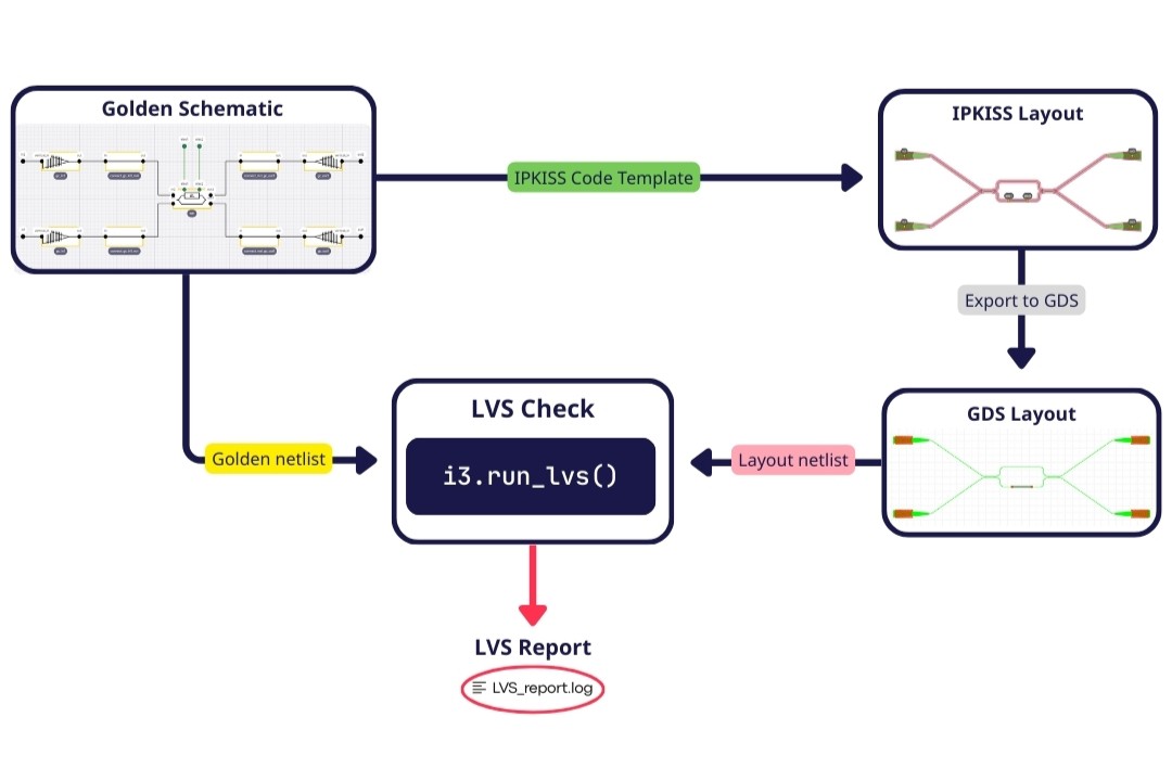
IPKISS LVS flow
In the image above you can see the LVS flow that is implemented in IPKISS. Let’s create a simple example circuit and follow this flow.
Step 1: Create a golden schematic in Canvas
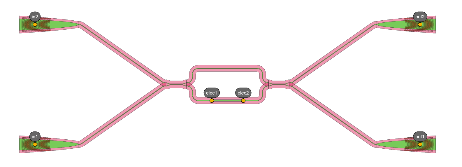
We will start by creating a golden schematic in Canvas. This schematic is considered “golden” as it represents the final design intent of the circuit.
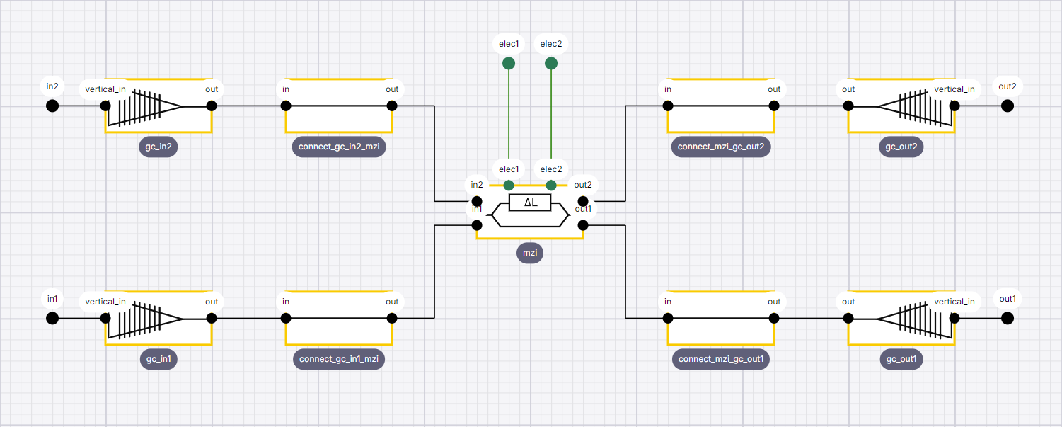
Golden schematic
The circuit consists of an MZI with optical I/O.
While creating the Canvas project we have imported the iclib file of both the SiFab demo PDK and the user library defined as the P-Team Library.
To create the circuit, we have used the MZI component from the P-Team Library and the grating couplers optimized for 1550 nm wavelength from the SiFab demo PDK.
For every connection between the circuit’s components we drag-and-drop a i3.RoundedWaveguide cell from the SiFab PDK.
Finally, we have added 4 optical external terms and 2 electrical terms to define the exposed ports of our circuit.
Note: In order to follow our current LVS flow, it is important to define a i3.RoundedWaveguide for every physical waveguide within your golden schematic.
Two directly linked components will be considered as joined components (as if you would use i3.Join functionality to connect them) during netlist comparison between layout and schematic.
Step 2: Generate layout code from golden schematic
Now that we have the final design intent, we can convert our schematic into a layout implementation in IPKISS’ code environment and finalize it.
If you right-click anywhere in your Canvas window, you can select Code Templates and choose one of our templates to get started on the layout implementation.
We will choose the i3.Circuit (i3.ConnectManhattan/i3.ConnectElectrical for LVS), as this template conveniently converts all the i3.RoundedWaveguide into i3.ConnectManhattan and also adds the method to perform the LVS check automatically at the end of the code.
You can find the generated code from canvas in 1_lvs_example.py.
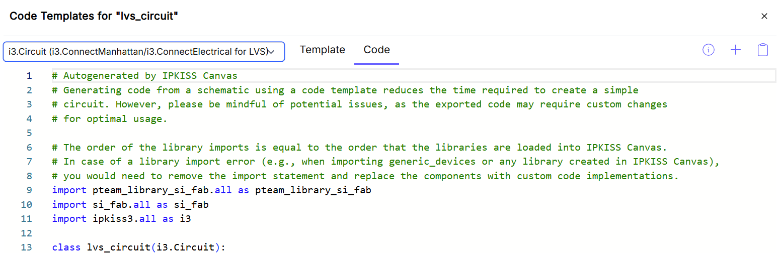
Code template of golden schematic
If we copy this template inside our editor and run the script we get the following layout visualisation.
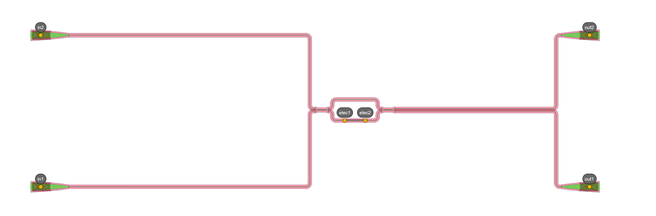
Layout visualization of code template
We are now free to adjust layout specifications inside our code such as the positions of the instances and the type of the connectors. From a design perspective it is important that the input and output waveguides connected to the MZI have the same length. In order to ensure this we will create a parametric circuit and define the spacing between our components parametrically.
Step 3: Export IPKISS layout to GDS-file
Inside 2_finished_layout.py you can find a finalized parametric layout.
Visualization of finished layout
import pteam_library_si_fab.all as pteam_library_si_fab
import si_fab.all as si_fab
import ipkiss3.all as i3
from pathlib import Path


class RoutedMZI(i3.Circuit):
    mzi = i3.ChildCellProperty(doc="MZI used in circuit")
    gc = i3.ChildCellProperty(doc="grating coupler used in circuit")
    spacing_x = i3.PositiveNumberProperty(default=100, doc="spacing between mzi and couplers in x-direction")
    spacing_y = i3.PositiveNumberProperty(default=50, doc="spacing between mzi and couplers in y-direction")

    def _default_mzi(self):
        return pteam_library_si_fab.MZI()

    def _default_gc(self):
        return si_fab.FC_TE_1550()

    def _default_insts(self):
        return {
            "mzi": self.mzi,
            "gc_in2": self.gc,
            "gc_in1": self.gc,
            "gc_out2": self.gc,
            "gc_out1": self.gc,
        }

    def _default_specs(self):
        return [
            # Optical connections
            i3.ConnectBend("gc_in1:out", "mzi:in1", "connect_gc_in1_mzi"),
            i3.ConnectBend("gc_in2:out", "mzi:in2", "connect_gc_in2_mzi"),
            i3.ConnectBend("mzi:out2", "gc_out2:out", "connect_mzi_gc_out2"),
            i3.ConnectBend("mzi:out1", "gc_out1:out", "connect_mzi_gc_out1"),
            # Placement specs
            i3.Place("mzi@C", (0, 0), angle=0),
            i3.Place("gc_in2", (-self.spacing_x, self.spacing_y), relative_to="mzi:in2", angle=0),
            i3.Place("gc_in1", (-self.spacing_x, -self.spacing_y), relative_to="mzi:in1", angle=0),
            i3.Place("gc_out2", (self.spacing_x, self.spacing_y), relative_to="mzi:out2", angle=180),
            i3.Place("gc_out1", (self.spacing_x, -self.spacing_y), relative_to="mzi:out1", angle=180),
        ]

    def _default_exposed_ports(self):
        return {
            "gc_in2:vertical_in": "in2",
            "gc_in1:vertical_in": "in1",
            "gc_out2:vertical_in": "out2",
            "gc_out1:vertical_in": "out1",
            "mzi:elec1": "elec1",
            "mzi:elec2": "elec2",
        }
We will convert this layout to a GDS-file by using the method i3.write_gdsii().
Inside this method we will set the parameter export_ports to True which allows us to create a GDS-file suitable for an LVS-check.
This code is already included in the code template.
if __name__ == "__main__":
    cell = RoutedMZI(name="lvs_example")
    cell_lo = cell.Layout()
    cell_lo.write_gdsii("finished_layout.gds", export_ports=True)
Step 4: Run LVS
Now we are able to do an LVS-check by comparing our golden netlist with the netlist of the finished layout.
For that we introduce the method i3.run_lvs() and pass the finalized GDS file as a parameter.
We also specify the the canvas schematic project, library and cell and the name of the log-file where the LVS report will be written to.
This code is automatically included in the code template as well.
By running i3.run_lvs() an LVS-check can now be executed.
    # Run LVS-check
    message = (
        "LVS check passed"
        if i3.run_lvs(
            gds_file="finished_layout.gds",
            schematic_file=schematic_file_path,
            canvas_library="library",
            canvas_cell="lvs_circuit",
            log_file="LVS_report.log",
            ignore_electrical=False,
        )
        else "LVS check failed, see the log file for details"
    )
    print(message)
After running 2_finished_layout.py we see a printed message stating that the LVS check has passed. The content of the LVS_report.log also shows no errors.

LVS_report.log
This indicates we have performed a succesful LVS check and are able to send the GDS file to the foundry!
Possible LVS errors
Let’s have a look what happens if we forget about a connection in our layout and run an LVS check. In 3_missing_connection.py we have commented out the first connector in the specs of our layout code to test this.
    def _default_specs(self):
        return [
            # Optical connections
            # i3.ConnectBend("gc_in1:out", "mzi:in1", "connect_gc_in1_mzi"),
            i3.ConnectBend("gc_in2:out", "mzi:in2", "connect_gc_in2_mzi"),
            i3.ConnectBend("mzi:out2", "gc_out2:out", "connect_mzi_gc_out2"),
            i3.ConnectBend("mzi:out1", "gc_out1:out", "connect_mzi_gc_out1"),
            # Placement specs
            i3.Place("mzi@C", (0, 0), angle=0),
            i3.Place("gc_in2", (-self.spacing_x, self.spacing_y), relative_to="mzi:in2", angle=0),
            i3.Place("gc_in1", (-self.spacing_x, -self.spacing_y), relative_to="mzi:in1", angle=0),
            i3.Place("gc_out2", (self.spacing_x, self.spacing_y), relative_to="mzi:out2", angle=180),
            i3.Place("gc_out1", (self.spacing_x, -self.spacing_y), relative_to="mzi:out1", angle=180),
        ]
Now let’s run the LVS-check and have a look at the written log-file:
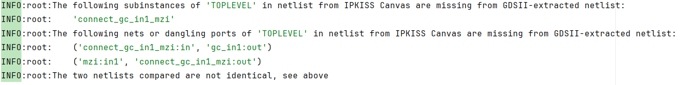
LVS_report_missing_connection.log
You can see that in the netlist from IPKISS Canvas (golden netlist) we now find a waveguide connection that is not found in the GDSII-extracted netlist from the layout. The same can be said for the nets linked to that waveguide connection. In this way every difference in name of instances, terms or nets between both of the netlists will be flagged and logged onto this file.
On top of that, it is required that the hierarchy remains consistent as also subinstances are compared with each other. For example, the MZI from the P-Team Library used in our schematic is a hierarchical component. All the subinstances of the MZI should remain identical to the ones used in the schematic in order to have a succesful LVS check.
Conclusion
We can conclude that running an LVS check is a necessary step to detect mistakes in the physical layout implementation and to feel more confident when submitting your design. All that is left to do is fix the errors from the generated log-file, so you can confidently send out your verified layout to the foundry!