Introduction
Application: 400G Ethernet
In this tutorial, we target a data communication application, specifically 400GBase-LR8 [3]. However, the design flow and principles can be equally applied to other applications as well. 400GBase-LR8 is an IEEE physical layer standard for 400 Gbit/s Ethernet over 10km or further. It uses 8 parallel wavelength channels with a coarse spacing (CWDM) at 50 Gbit/s each.
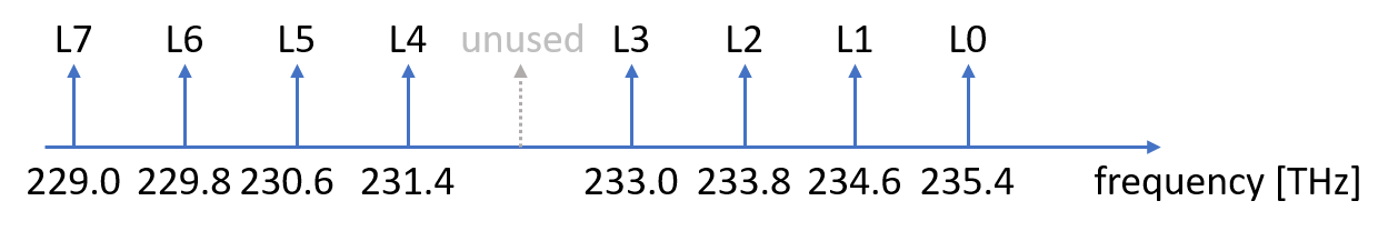
In the transmitter optical sub-assembly (TOSA) and receiver optical sub-assembly (ROSA) for such a system, 8-channel multiplexing (mux) and demultiplexing (demux) components are needed, respectively. The channels are coarsely spaced across the O-band (1260-1360 nm), using a step of 800 GHz around a center frequency of 232.2 THz. The center frequency itself is unused. In this tutorial, we will design an AWG so that it meets these specifications and we will prepare it for tape-out and further re-use within a circuit design.
Lane |
Center frequency (THz) |
Center wavelength (nm) |
Wavelength range |
|---|---|---|---|
L0 |
235.4 |
1273.55 |
1272.55 to 1274.54 |
L1 |
234.6 |
1277.89 |
1276.89 to 1278.89 |
L2 |
233.8 |
1282.26 |
1281.25 to 1283.28 |
L3 |
233.0 |
1286.66 |
1285.65 to 1287.69 |
L4 |
231.4 |
1295.56 |
1294.53 to 1296.59 |
L5 |
230.6 |
1300.05 |
1299.02 to 1301.09 |
L6 |
229.8 |
1304.58 |
1303.54 to 1305.63 |
L7 |
229.0 |
1309.14 |
1308.09 to 1310.19 |
Project structure
In this tutorial, we will go through the following flow:
Review the AWG subcomponents
We will generate and review the subcomponents of our AWG to make sure that they do what we want them to do. We will use the subcomponents from SiFab
Synthesise the AWGs
We we will start from high-level specifications, including the functional specifications we have described above. From this, we will derive the implementation parameters of our AWG.
Finally, the AWG is assembled based on these implementation parameters: first the star couplers and then the full AWG.
Implement the AWG Layout
Then, we will implement the layout of our awg from the implementation parameters we have defined.
Simulation and analysis
Next, we will simulate our AWG and create an analysis report including information such as cross-talk and insertion loss.
AWG finalization.
Finally, we will fix DRC errors and route our AWG to grating couplers
When reviewing our subcomponents, we will run separate example files for them one-by-one.
However, for ease of learning, we will go through all the remaining part flow in a single script.
You can find this script in the path luceda_academy/training/topical_training/design_awg/example_generate_awg.py.
We will refer to this example throughout this tutorial.