PhaseShifterWaveguideTemplate
- class picazzo3.modulators.phase.trace.PhaseShifterWaveguideTemplate
Generic phase shifter waveguide trace template. When extruded into a (straight) waveguide, this template draws the necessary implant, contact and metallization layers on top of the underlying waveguide template. This waveguide template should be specified in the “trace_template” property.
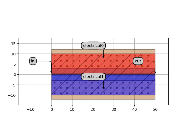
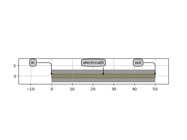
This PCell can be used for several types of phase shifters, for example: * P(I)N junction injection or depletion phase shifters, with P and N implants, contacts and metal on two sides * Thermal phase shifters using a metal heater on top * Thermal phase shifters using an implanted waveguide
At the Layout level, windows can be specified separately for the implants (the silicon level), contacts (pre-metal/contact level) and the metallization (e.g. metal1 level). Just fill or leave open each of the three sets of windows, and use them to implement the desired type of phase shifter.
Subclass this PCell to create specialized phase shifters, and add electrical ports.
- Parameters:
- trace_template: PCell and _TraceTemplate
Refers to the other trace template from which information is taken to build this trace template.
- name: String that contains only ISO/IEC 8859-1 (extended ASCII py3) or pure ASCII (py2) characters
The unique name of the pcell
Views
- class Layout
- Parameters:
- metal_windows: List with type restriction, allowed types: <class ‘ipkiss3.pcell.trace.window.window._TraceWindow’>
List of Trace Windows for the metallization layers
- contact_windows: List with type restriction, allowed types: <class ‘ipkiss3.pcell.trace.window.window._TraceWindow’>
List of Trace Windows for the contacts
- implant_windows: List with type restriction, allowed types: <class ‘ipkiss3.pcell.trace.window.window._TraceWindow’>
List of Trace Windows for the implant layers
- windows_for_ports: List with type restriction, allowed types: <class ‘ipkiss3.pcell.trace.window.window._TraceWindow’>
List of Trace Windows from which ports will be generated
- core_width: float and number > 0
width of the waveguide core
- core_layer: __Layer__
layer used to define the core of the waveguide
- flatten_contents:
if True, it will insert the referred trace as elements in the layout, rather than as an Instance
- pin_shape: Shape
shape to be used for the pins
- trace_template_for_ports: _TraceTemplate.Layout
Trace template to be used for the ports. Default = this template
- windows: List with type restriction, allowed types: <class ‘ipkiss3.pcell.trace.window.window._TraceWindow’>
List of Trace Windows to draw on top of the already defined TraceTemplate
- keep_original_trace_template:
- width: float and int, float, integer, floating and number >= 0
- control_shape_layer: __Layer__
layer on which the control shape is drawn
- draw_control_shape:
draws the control shape on top of the waveguide
- cover_layers: List with type restriction, allowed types: <class ‘ipkiss.primitives.layer.Layer’>
layers that can be used to generate additional coverage of the trace (e.g. manhattan corners)
- view_name: String that contains only alphanumeric characters from the ASCII set or contains _$. ASCII set is extended on PY3.
The name of the view
Examples
import si_fab.all as pdk  # noqa: F401
import ipkiss3.all as i3
from picazzo3.modulators.phase import PhaseShifterWaveguideTemplate
from picazzo3.traces.rib_wg import RibWaveguideTemplate
from picazzo3.electrical.contact import ContactHole

wire_t = RibWaveguideTemplate()
wire_t.Layout(core_width=0.9, cladding_width=2 * i3.TECH.WG.TRENCH_WIDTH + 0.9)

c = ContactHole(name="PNPS_CONT")
c.Layout()

contact_windows = [
    i3.PeriodicArrayReferenceTraceWindow(
        reference=c, offset=-4.0 - 2.5 * i, exclude_ends=(0.5 * 3.0, 0.5 * 3.0), pitch=3.0
    )
    for i in range(3)
]

contact_windows += [
    i3.PeriodicArrayReferenceTraceWindow(
        reference=c, offset=4.0 + 2.5 * i, exclude_ends=(0.5 * 3.0, 0.5 * 3.0), pitch=3.0
    )
    for i in range(3)
]

implant_windows = [
    i3.PathTraceWindow(layer=i3.TECH.PPLAYER.P, start_offset=0.0, end_offset=10.0),
    i3.PathTraceWindow(layer=i3.TECH.PPLAYER.N, start_offset=0.0, end_offset=-10.0),
]

metal_windows = [
    i3.PathTraceWindow(layer=i3.TECH.PPLAYER.M1, start_offset=3.0, end_offset=12.0),
    i3.PathTraceWindow(layer=i3.TECH.PPLAYER.M1, start_offset=-3.0, end_offset=-12.0),
]

ps_t = PhaseShifterWaveguideTemplate(trace_template=wire_t)
ps_t.Layout(contact_windows=contact_windows, implant_windows=implant_windows, metal_windows=metal_windows)

ps = ps_t(name="TestPhaseShifterWaveguideTemplate1")
ps_lay = ps.Layout(shape=[(0.0, 0.0), (50.0, 0.0)])
ps_lay.visualize(annotate=True)

import si_fab.all as pdk  # noqa: F401
import ipkiss3.all as i3
from picazzo3.modulators.phase import PhaseShifterWaveguideTemplate
from picazzo3.traces.rib_wg import RibWaveguideTemplate

wire_t = RibWaveguideTemplate()
wire_t.Layout(core_width=0.9, cladding_width=2 * i3.TECH.WG.TRENCH_WIDTH + 0.9)

metal_windows = [i3.PathTraceWindow(layer=i3.TECH.PPLAYER.M1, start_offset=-1.0, end_offset=1.0)]

ps_t = PhaseShifterWaveguideTemplate(trace_template=wire_t)
ps_t.Layout(metal_windows=metal_windows)

ps = ps_t(name="TestPhaseShifterWaveguideTemplate2")
ps_lay = ps.Layout(shape=[(0.0, 0.0), (50.0, 0.0)])
ps_lay.visualize(annotate=True)
