Thermal Crosstalk Analysis in PIC Switch Networks
Optical switch networks are essential circuits used for routing optical signals in applications ranging from telecommunications to quantum computing and artificial intelligence. These designs are typically built by cascading smaller, fundamental switching units and their performance can be heavily influenced by thermal crosstalk. In order to design these switches it is essential that we have tools to simulate and optimize their behavior accurately.
In this tutorial we will demonstrate a data-driven workflow to analyze and mitigate thermal crosstalk in PIC switch networks using the IPKISS parametric design framework and Luceda’s Circuit Analyzer.
The full project of this application example can be found in the Luceda Academy training materials folder: topical_training/benes_switch_circuit_analyzer/thermal_crosstalk.
Layout-aware variability analysis using Circuit Analyzer
While a nominal simulation provides a baseline for the switch’s behavior, the real-world performance of photonic integrated circuits is sensitive to manufacturing process variations and operating conditions. For instance, variations in waveguide width or temperature can significantly impact the behavior of components like MZI switches.
In the last tutorial a corner analysis of component model parameters allowed designers to explore the performance sensitivity to process variations. Now we will leverage Circuit Analyzer again to optimize the same circuit with a focus on modelling temperature variations and performing a layout-aware variability analysis.
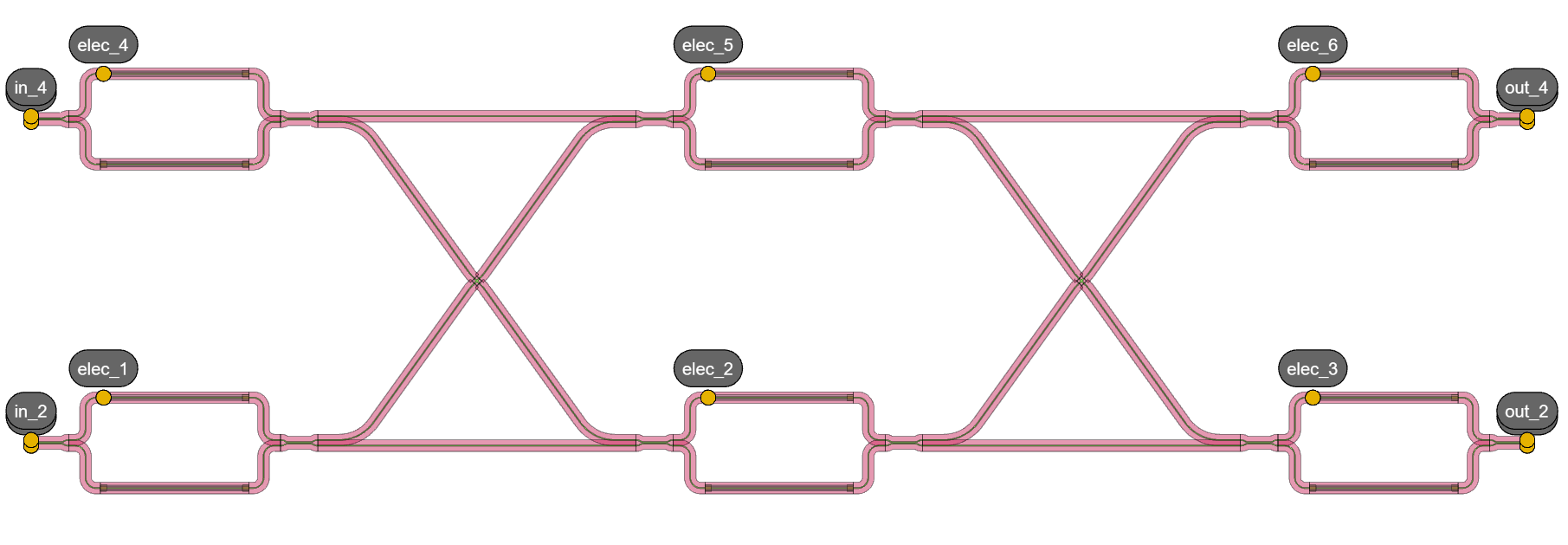
Layout of a 4x4 switch with a Benes architecture.
Component thermal variability
The components used for these circuits are taken out of a specific user library pteam_library_thermal created to specifically model thermal crosstalk. Inside this library you can find the components, models, the variability configuration for Circuit Analyzer and specific types of switch circuits that can be analyzed. Let’s have a look at how thermal variability is modeled for the individual components of our 4x4 switch:
Waveguides: The waveguides in the MZI arm will undergo a phase shift due to refractive index variations caused by temperature changes. This effect is defined inside
models.pyand modeled by including a temperature-dependent term in the waveguide’s effective index model.Crossings: These components are also affected by temperature. We have simulated them at two different temperatures (0K and 50K above the nominal temperature) and stored the results in touchstone files carrying S-matrix data. Circuit Analyzer can use this data to interpolate the component’s behavior at any temperature within this range. The variability is defined through the yaml-file by directly interpolating between the touchstone files.
Directional couplers: Similarly as the crossings we have S-matrix data for the two different temperatures. The variability is defined in
models.pywhere a phase relationship between inputs and outputs is enforced to avoid phase wrapping errors.Phase shifter: The phase shifter itself does not have any variability defined inside its model.
The variability model for our components is defined inside the following Circuit Analyzer configuration files: models.yaml and models.py.
models.yaml:
version: 1
libraries:
  si_fab:
    cells:
      GenericWaveguide:
        generate_parameters: "models.waveguide_parameters"

  pteam_library_thermal:
    cells:
      ThermalDC50:
        generate_parameters: "models.dc_50"

      ThermalCrossing:
        filename_format: "../components/crossing/data/smatrix_{T}.s4p"


global_parameters:
  T:
    doc: "Temperature"
    default: 0
    corners: [ 0, 50 ]
models.py:
# Copyright (C) 2020-2025 Luceda Photonics


import numpy as np
import ipkiss3.all as i3
import pteam_library_thermal.all as pt_lib
import os
import circuit_analyzer as ca


def waveguide_parameters(self, **parameters):
    """This method is called by Circuit Analyzer. Depending on the simulation strategy:

    - Corner Analysis: it will call it for each corner, where parameters contains the corner values
    - Monte Carlo: it will call for each sample, where parameters are sampled from a distribution
    - Location-Aware Variability Analysis: it will call for each sampled point on the wafer/die,
      where parameters are taken from the wafer map.

    """
    template = self.template
    # Here we can calculate the n_eff as function of wafer thickness.
    core_height = template.core_height
    core_width = template.cell.get_default_view(i3.LayoutView).core_width
    neff_fit_coeffs = template.get_n_eff_interp_for_design_parameters(core_width, core_height)

    thermo_optic_coefficient = 1.8e-4
    delta_neff = thermo_optic_coefficient * parameters["T"]
    neff_fit_coeffs[-1] = neff_fit_coeffs[-1] + delta_neff

    return {
        "n_eff": np.array(neff_fit_coeffs),
    }


def dc_50(self: pt_lib.ThermalDC50, **parameters):
    """This method is called by Circuit Analyzer. Depending on the simulation strategy:

    - Corner Analysis: it will call it for each corner, where parameters contains the corner values
    - Monte Carlo: it will call for each sample, where parameters are sampled from a distribution
    - Location-Aware Variability Analysis: it will call for each sampled point on the wafer/die,
      where parameters are taken from the wafer map.

    The SMatrix data from FDTD simulations is read and interpolated. A fixed phase relationship
    between the phases of output ports is enforced, to avoid phase unwrapping-related inconsistencies
    """

    path_dc = os.path.join(
        os.path.dirname(os.path.dirname(os.path.abspath(__file__))), "components", "dir_coupler", "data"
    )
    results = ca.fab_corner_variability.fab_params_to_model_params_interpol_bspline(
        circuit_model=self, filename_format=os.path.join(path_dc, "smatrix_{T}.s4p"), **parameters
    )
    # Adding a phase offset to transmission from port 0 (in0) to port 3 (out1)
    results["c_phase"][0, 3, :] = results["c_phase"][0, 2, :] + np.pi / 2
    results["c_phase"][3, 0, :] = results["c_phase"][2, 0, :] + np.pi / 2
    # Adding a phase offset to transmission from port 1 (in1) to port 2 (out0)
    results["c_phase"][1, 2, :] = results["c_phase"][1, 3, :] + np.pi / 2
    results["c_phase"][2, 1, :] = results["c_phase"][3, 1, :] + np.pi / 2

    return results
Now we can simulate the 4x4 switch at different temperatures and see how its performance changes.
Self-heating in an MZI switch and voltage optimization
Let’s take a step back and have a look at a single 2x2 switch. When a voltage is applied to the heater, not only does the phase of the waveguide directly beneath the heater change, but the waveguides around it are also impacted by the heat. This is known as “self-heating” in the 2x2 switch, which can impact the performance of the circuit.
We can simulate this effect by creating a thermal profile of the heated phase shifter and using Circuit Analyzer to superimpose it over the circuit layout. For this tutorial a fictional thermal map is used to represent the temperature variations caused by the phase shifter. It could be replaced by data from a thermal solver or an experimental setting.
The script below simulates a 2x2 switch with the thermal profile taken into account.
import si_fab.all as pdk
import pteam_library_thermal.all as pt_lib
import os
import numpy as np
from util_files.ca_utils import create_thermal_profile, visualize_profiles
import circuit_analyzer.all as ca


if __name__ == "__main__":
    # Get the cross and bar voltages
    v_bar, v_cross = np.loadtxt(
        os.path.join(os.path.dirname(pt_lib.__file__), "circuits", "switch_2x2", "pcell", "switch_voltage_biases.txt"),
    )

    # Initialize the Switch PCell
    cell = pt_lib.SwitchMZI2x2(y_spacing=6, vdiff=v_bar)
    wavelengths = np.linspace(1.5, 1.6, 501)
    cell_cm = cell.CircuitModel()
    S_nominal = cell_cm.get_smatrix(wavelengths=wavelengths)

    # Create thermal map
    pdk.SiWireWaveguideTemplate.CircuitModel.VE_sampling_period = 2
    thermal_map, x_positions, y_positions, profile, X_tot, Y_tot = create_thermal_profile(cell)
    visualize_profiles(cell_cm, profile, X_tot, Y_tot)

    # Circuit Analyzer code
    # Superimpose thermal map over circuit and calculate response
    config_root = os.path.join(os.path.dirname(pt_lib.__file__), "variability_info")
    with ca.setup(
        config_path=config_root,
        config_filename=os.path.join(config_root, "models.yaml"),
    ):
        smats = ca.sweep_wafermap(
            circuit_model=cell_cm,
            wavelengths=wavelengths,
            deviation_maps={
                "T": thermal_map,
            },
            positions=[(0, 0)],
        )
        smats.append(S_nominal)

    term_pairs = [("in_1", "out_2")]
    ca.visualize_smatrices(smats[::-1], term_pairs=term_pairs)
The thermal profile of the heated waveguide is shown below, overlaid on the circuit layout.
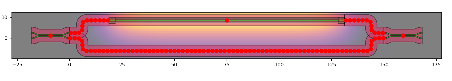
Thermal profile of the 2x2 MZI switch when a voltage is applied to the heater.
It will then visualize the crosstalk of the 2x2 switch with and without the self-heating effect. Taking self-heating of the switch into consideration seems to increase the crosstalk to values higher than -20dB.
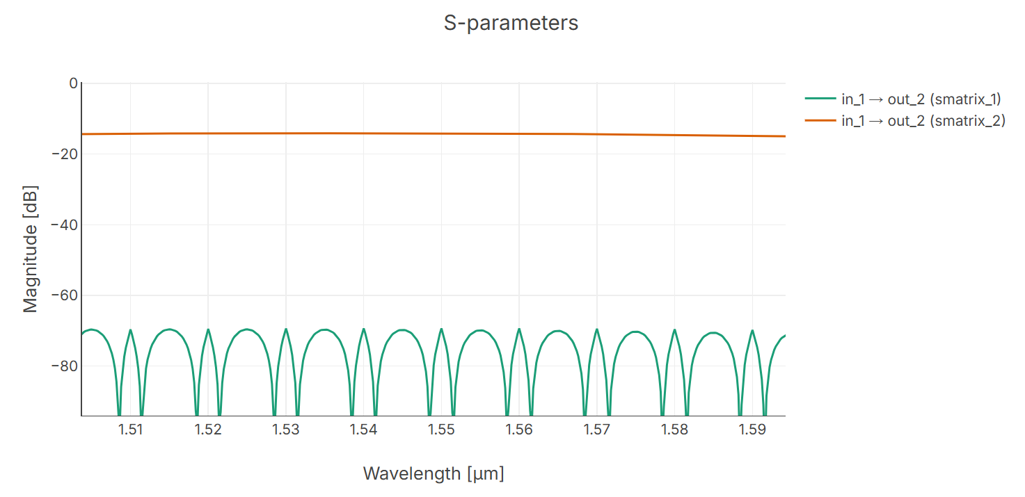
Crosstalk between in_1 and out_2 port with and without self-heating (smatrix_1 and smatrix_2 respectively)
The self-heating effect changes the optimal voltage required to achieve the bar state (maximum transmission to the through port). We can find the new optimal voltage by running an optimization sweep. The following script sweeps the MZI arm spacing, and for each spacing value, it finds the optimal voltage that minimizes the crosstalk at the target wavelength.
Run thermal_profile_simulation/2_sweep_mzi_height_and_get_opt_voltages.py to find the new optimal voltage by running an optimization sweep.
The plot below shows the optimized voltage as a function of the MZI arm spacing.
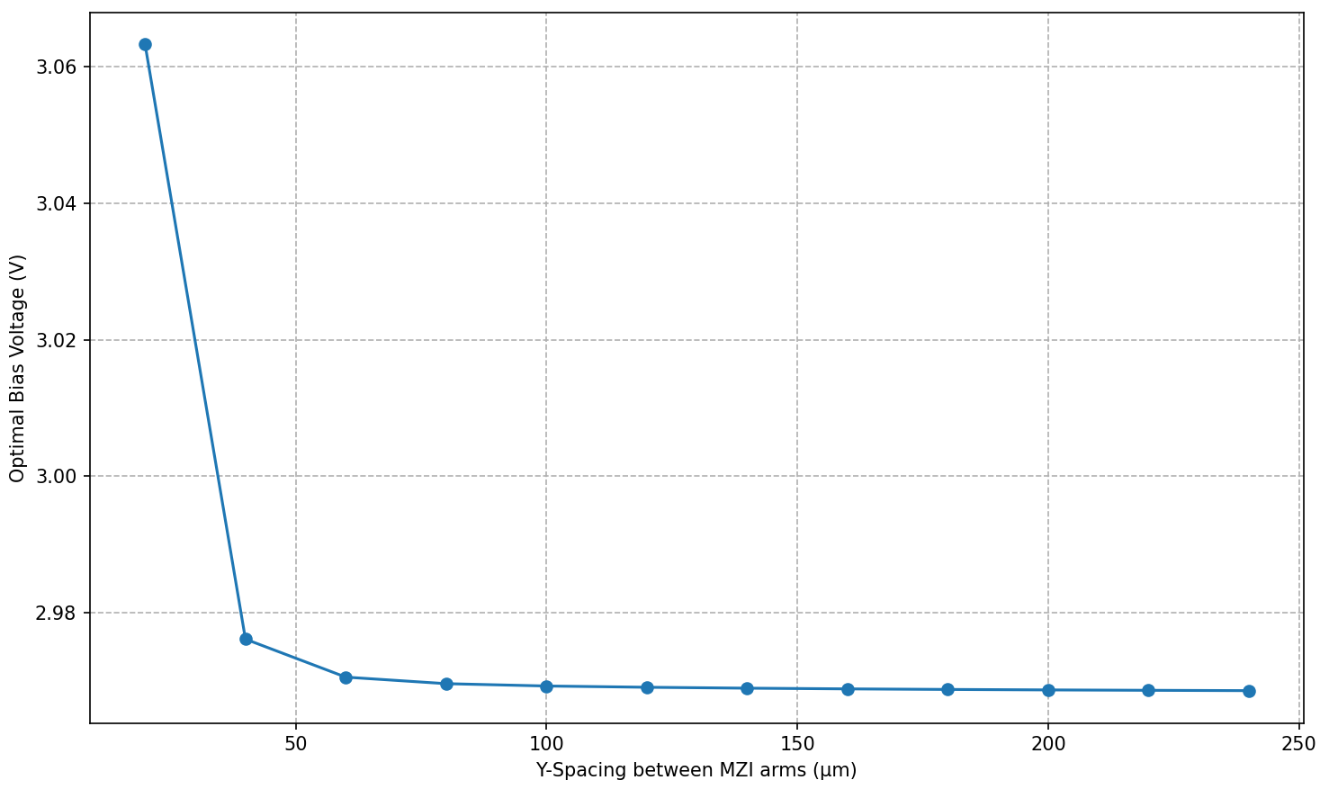
Optimized voltage as a function of MZI arm spacing, taking into account self-heating effects.
Using the optimized voltage as a bias will now result into a significant reduction of the crosstalk in the 2x2 switch.
Thermal crosstalk in switch networks
In a dense switch network, the heat from one MZI can affect the performance of its neighbors. This is known as thermal crosstalk.
Let’s run thermal_profile_simulation/3_switch_4x4_loss_and_crosstalk_with_thermals.py to simulate the 4x4 switch with a thermal profile that includes the contributions from all active heaters.
It creates a thermal map of the entire circuit and uses Circuit Analyzer to calculate the S-matrix of the entire circuit.
You can see how the heat from the active heaters spreads to the neighboring switches.
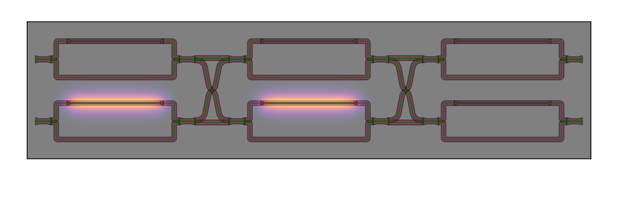
Thermal profile of the 4x4 Benes switch with bias state [0,0,1,1,1,1].
Design sweep over 3 dimensions
To find an optimal and robust design, we need to evaluate the switch’s performance not just in one state, but across all possible configurations and a range of geometries. A simple 2D sweep is insufficient because the thermal crosstalk profile changes dramatically with each routing path. We therefore perform a comprehensive 3D sweep over the following parameters:
MZI height: The spacing between the arms of the constituent 2x2 MZI switches. A larger spacing can reduce self-heating effects but increases the MZI’s footprint.
Switch vertical spacing: The vertical gap between the parallel rows of 2x2 switches in the 4x4 layout.
Bias state: The routing configuration of the switch. A 4x4 Benes switch has 24 possible permutations (routing states), each with a unique thermal profile and performance.
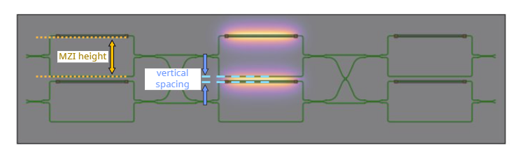
Design sweep parameters
In order to do a full analysis we systematically iterates through every combination of these three parameters. For each point in this design space, we will performs a full layout-aware simulation with Circuit Analyzer and calculate the following key metrics:
Worst-case Insertion Loss (IL): The highest signal loss on any of the four desired input-output paths.
Worst-case Crosstalk (XT): The strongest unwanted signal that leaks to an incorrect output port.
Port Flip: A critical failure where thermal detuning is so severe that a switch routes the signal to the wrong output entirely.
The script 4_switch_4x4_sweep_3d.py is configured to run a minimal parameter sweep for a certain amount of devices.
To generate the comprehensive dataset used for the analysis in this tutorial (3d_sweep_results.csv inside the data folder of this project), you will need to modify the script to broaden the sweep ranges.
The script 5_plot_sweep_results.py processes the raw data.
For each geometric configuration (a combination of MZI height and vertical spacing), it aggregates the results from all 24 bias states to find the absolute worst-case IL and XT.
This tells us the performance boundaries for that specific geometry, regardless of how the switch is configured.
The results are visualized as 2D heatmaps. Worst-case crosstalk (left) and insertion loss (right) is shown as a function of MZI height and switch vertical spacing. Each cell is annotated with its performance and a symbol indicating whether port flips occurred (X) or not (✓) for that geometry across all 24 bias states.
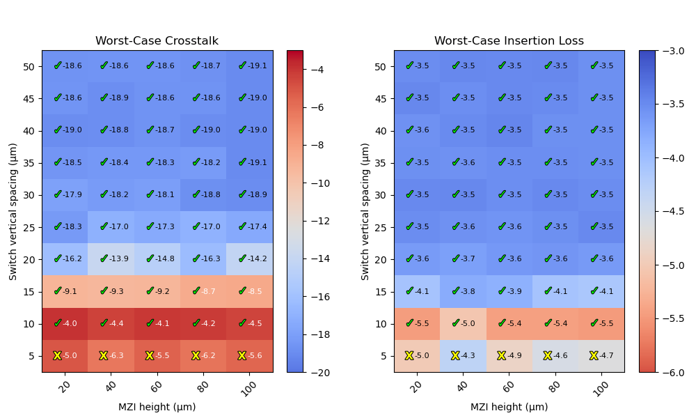
3D sweep results for worst-case crosstalk and insertion loss.
Crosstalk versus area and footprint constraints
While performance is critical, chip area is also a major constraint.
The script 6_plot_sweep_results_with_area.py extends the analysis by calculating the total PIC area for each geometric configuration.
It then generates the same heatmaps but adds a visual overlay to gray out designs that exceed a specified area budget (e.g., 0.05 mm²).
This final visualization allows a designer to quickly identify the optimal trade-off between performance and footprint. For a given area constraint, one can easily locate the design with the lowest crosstalk and insertion loss that is guaranteed to be free of port-flip errors.
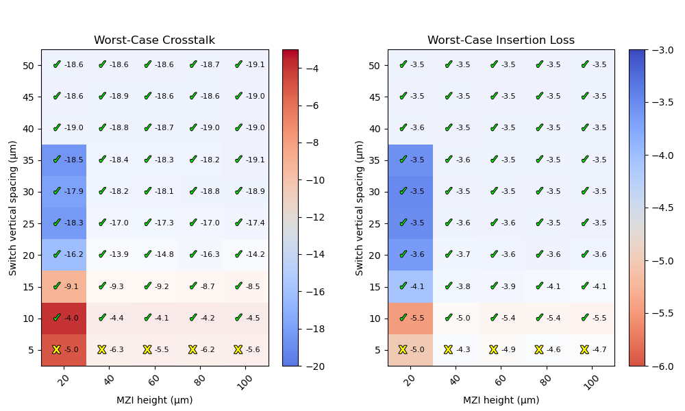
Worst-case performance plots with a footprint constraint.
Finally, we can plot the worst-case crosstalk as a function of the total PIC area. This allows us to assess the trade-off between performance and footprint.
Let’s run thermal_profile_simulation/7_plot_crosstalk_versus_area.py to plot this relationship.
It shows that for a given MZI height, the crosstalk improves as the area increases, which is expected as the switches are spaced further apart.
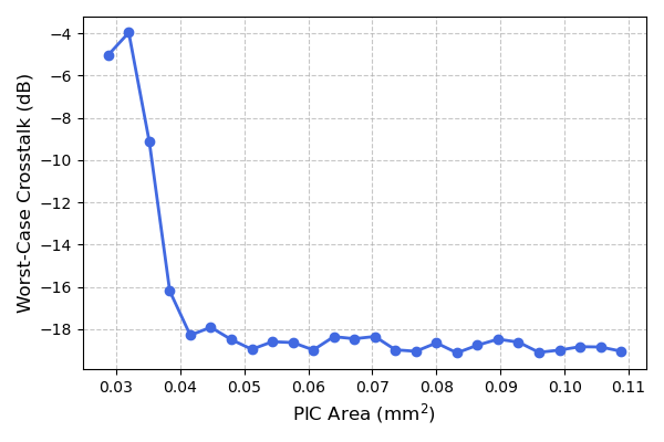
Worst-case crosstalk as a function of the total PIC area for a fixed MZI height of 20 um.
Test your knowledge
Now it is up to you to try out our tools yourself and have a deeper look at the circuits inside the library in this project:
4x4 Spanke-Beneš switch: What is the advantage of using Spanke-Beneš switches in terms of thermal crosstalk? Can you reduce the thermal crosstalk further using a similar footprint area as previously discussed 4x4 switch?
8x8 switch: How would you approach optimizing thermal crosstalk for the 8x8 switch inside the library?