PDK development: Cornerstone Ge-on-Si
In this tutorial, we will create a Process Design Kit (PDK) using the Luceda platform.
A Process Design Kit (PDK) is a collection of technology definitions, design rules, documentation, and component libraries provided by a fabrication facility (Fab or Foundry) to enable designers to create manufacturable circuits for a specific process. It serves as the interface between the designer, the fabrication process, and the design automation software (e.g., Luceda IPKISS), encompassing technology definitions (layers and processes), design rules, simulation models, and tool-specific configuration settings.
Official PDKs supported by Luceda are listed here.
The goal of this tutorial is to build a functional PDK from scratch. You will learn how to:
Define the technology according to foundry specifications
Create basic PCells (Parametric Cells)
Automate the generation of documentation and technology files for a distributable PDK
This workflow is important because it accelerates PDK development and simplifies maintenance. It enables both high-volume foundries and prototyping facilities to efficiently create, customize, and distribute PDKs that are intuitive and easy to use for designers.
We selected the Cornerstone Ge_on_Si (Germanium-on-Silicon) process for this tutorial because it is publicly accessible and has a relatively simple layer stack. This makes it an ideal starting point for learning the fundamentals of PDK construction. While the si_fab demo PDK is more comprehensive, its complexity may be overwhelming for readers new to PDK development.
Note
Luceda PDKs for the Cornerstone Si and SiN processes are available in the Luceda Control Center (LCC) under the Design Kits tab.
1. Initializing the Ge-on-Si development project from LCC
The first step is to generate a PDK template, which provides the initial folder structure and configuration files. To create this template, launch LCC, navigate to the Design Kits tab, and click New Design Kit Project.
A dialog will appear prompting you to enter the project details. Hover over the dot symbol next to each field to view a tooltip description. Fill in the fields as follows:
- Import Name:
- The name used for Python imports.Constraints: letters, numbers, and underscores only. Cannot start with a number.
- Display Name:
- The display name used in documentation.Note: spaces and capitalization are allowed.
- Company Name:
- The name of the organization creating the PDK.
- Target Location:
- The directory where the new project subfolder will be created.
- Version:
- The initial version, using Semantic Versioning format.
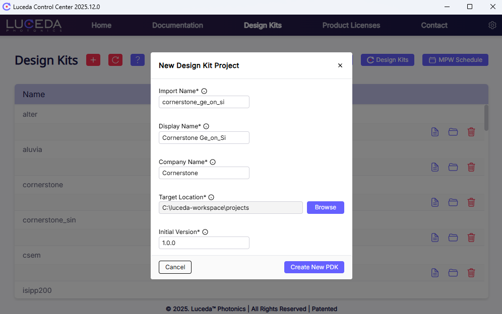
New Design Kit Project
Click Create New PDK. Then:
- If PyCharm is installed:
A new PyCharm project opens automatically. The Python interpreter should be configured automatically (visible in the bottom-right corner).
Note
If you are using PyCharm and the interpreter is not set, refer to Create a new IPKISS design project.
- If PyCharm is not installed:
The project folder opens in Windows Explorer.
The generated PDK template has the following folder structure. In the next sections, we will explain how to modify this template and adapt it to the actual process.
cornerstone_ge_on_si
├── cornerstone_ge_on_si
│   ├── docs
│   │   ├── examples
│   │   └── source
│   ├── cornerstone_ge_on_si.cfg
│   ├── iclib_export.yaml
│   └── ipkiss
│       └── cornerstone_ge_on_si
│           ├── components
│           ├── technology
│           ├── __init__.py
│           └── all.py
├── build.py
├── inspect_pdk.py
├── README.md
├── .gitattributes
├── .gitignore
└── .idea
2. Explore the template
The generated project is a functional template intended to accelerate development. It includes example layers, waveguides, placeholder components, and preconfigured documentation.
Inside the project (e.g., in PyCharm), begin by reviewing the README file.
Try the following run configurations to better understand the template:
- Inspect the PDK:
- Executes the script cornerstone_ge_on_si/inspect_pdk.py.The script prints all currently defined layers, components, and trace templates to the console.It also opens the Luceda Layout Visualizer to display these elements graphically.
- Build the PDK:
- Executes the script cornerstone_ge_on_si/build.py.This script generates a distributable version of the PDK.The resulting package is stored in the builds/ directory.The generated .zip file can be distributed to designers and installed directly via LCC.
Beyond the technology settings and components you implement manually, the build script automatically generates several key files based on the available data:
Documentation (PDF and HTML)
.lyp file for KLayout
layermap.txt file
.iclib file containing component definitions used for schematic-driven design in IPKISS Canvas. This library enables LVS (Layout Versus Schematic) consistency checks, SDL (Schematic-Driven Layout) workflows, and circuit-level simulation by exposing component symbols, ports, and connectivity metadata.
3. Configure PDK Metadata
This file is prefilled with the names provided in Step 1. You can update the version number here for future releases.
- PDK:
General metadata (name, description, license).
# config file for cornerstone_ge_on_si
---
PDK:
    name: Cornerstone Germanium-on-Silicon
    description: |
        Germanium-on-Silicon Process Design Kit
    version: 1.0.0
    date: 2026-01-27
    license:
        title: Cornerstone

# technology settings
Technology:
    location: cornerstone_ge_on_si/technology
- Exports:
Specifies which artifacts are included in the final distributable PDK. The primary exports include documentation (PDF and HTML), the .lyp file for KLayout, the layermap.txt file, and the .iclib file.
These files are stored in the following directories of the built PDK:
- Documentation:builds/cornerstone_ge_on_si/docs
- .lyp file for KLayout:builds/cornerstone_ge_on_si/techfiles/klayout/cornerstone_ge_on_si.lyp
- layermap.txt for OpenAccess:builds/cornerstone_ge_on_si/techfiles/klayout/layermap.txt
- .iclib file for schematic functionality:builds/cornerstone_ge_on_si/ipkiss/cornerstone_ge_on_si/cornerstone_ge_on_si.iclib
Exporters that are not required (e.g., OpenAccess or Tanner) can be commented out if the corresponding licenses are unavailable.
Within the Exports block, the files section allows you to include supplementary resources such as design examples. For each additional file, both a source and destination path must be defined. For example, if design examples are stored in docs/example in the development environment and should be preserved in the distributed PDK, they can be mapped accordingly.
# Remove the exporters that are not relevant for you
Exports:
    ipkiss:  # copies ipkiss files in the correct location
    documentation:
        formats:
            - pdf
            - html
    lyp:  # exports a lyp file that can be imported in KLayout
    layermap:  # exports a layermap.txt file, which can be loaded in other EDA tools
    gdsii:  # will automatically add fixed layoutviews to GDS-files in the 'gdsii' directory of the PDK.
    zip:  # generate a zip file
    iclib:  # automatically generate an .iclib file with symbols to be used in the IPKISS Canvas schematic editor.
            # default export settings can be changed in the iclib_export.yaml file
    # The openaccess exporter requires a license for the Link for Siemens EDA
    # If you have such a license, the next two lines can be uncommented
    # openaccess:  # only required when you need an openaccess enabled PDK.
    #     with_display: Yes
    # The tanner exporter requires a license for the Link for Siemens EDA
    # If you have such a license, the next line can be uncommented
    # tanner:  # only required for loading in Siemens L-Edit
    files:
        # copies additional files into the PDK
        - src: docs/examples
          dst: docs/examples
4. Technology and process definition
The technology configuration defines the physical process, materials, GDS mapping, visualization rules, design rules, and general settings that remain consistent across designs built with the PDK.
Extensive comments are provided throughout the file to help customize the process definition. Once the configuration is finalized, these comments can be removed to keep the file clean.
In tech.yaml, only certain blocks are strictly mandatory. For optional sections, IPKISS provides default values when they are omitted, allowing faster generation of an initial PDK version.
This file is organized into four main sections to structure the technology configuration:
Layers and purposes:
layers (mandatory): Defines a list of unique layer names (e.g., Ge_Etch1_LF, Floorplan). Each entry requires a name.
# The list of layers
# A layer is defined by
# - name: The unique name of the layer. Case matters.
# - doc [optional]: Description for the layer.
# - number [optional]: The layer number. Will be auto-generated if absent.
layers:
  - {name: Ge_Etch1_LF, doc: 1.8 um+-200nm Ge etch to define rib waveguides. Layer will be protected.}
  - {name: Ge_Etch1_DF, doc: 1.8 um+-200nm Ge etch to define rib waveguides. Layer will be etched.}
  - {name: Bleed, doc: 35-um-wide area at the edges of the design area for dicing streets.}
  - {name: Floorplan, doc: Cell outline}
  - {name: Label, doc: Labels (dark)}
  - {name: FinalChipSize, doc: Layer for indicating the Size of chip after dicing (size in x and y).}
  - {name: Text, doc: Text layer}
  - {name: DevRec, doc: Device recognition layer}
  - {name: PinRec, doc: Optical port (pin) recognition layer}
  - {name: PinRecM, doc: Electrical port recognition layer}
  - {name: FbrTgt, doc: Fiber ports on grating couplers (Fiber Target)}
  - {name: None, doc: No specific process}
Optional layer attributes include:
- doc: description used in automated documentation generation
- number: only required when supporting OpenAccess EDA tools
- purposes (optional): Defines the intent of a drawing (e.g., DOC, TRACE).This becomes mandatory when supporting OpenAccess EDA tools.If omitted, the
DRAWINGpurpose is implicitly used. - lpps (optional): Defines Process–Purpose Layer pairs.This is also mandatory for OpenAccess EDA support.
For this PDK, purposes and lpps are not required, so these sections remain unchanged.
GDSII mapping (mandatory):
This mapping ensures that each PPlayer in IPKISS corresponds to a specific (Layer, Datatype) pair in the GDSII file. Without this mapping, layers will be ignored during export.
# Configuration for GDS file export.
gds:
  # Mapping of layer names to GDS layer and datatype numbers.
  # number: A pair of the GDS layer number and the GDS datatype number.
  layer_table:
    - {lpp: Ge_Etch1_LF, number: [303, 0]}
    - {lpp: Ge_Etch1_DF, number: [304, 0]}
    - {lpp: Bleed, number: [98, 0]}
    - {lpp: Floorplan, number: [99, 0]}
    - {lpp: Label, number: [100, 0]}
    - {lpp: FinalChipSize, number: [99, 1]}
    - {lpp: Text, number: [66, 0]}
    - {lpp: DevRec, number: [68, 0]}
    - {lpp: PinRec, number: [1, 10]}
    - {lpp: PinRecM, number: [1, 11]}
    - {lpp: FbrTgt, number: [81, 0]}
You can also define GDS export settings such as cut_path and max_vertex_count:
  # GDS export options
  # export_options:
  #   cut_path: true # Whether to cut paths.
  #   path_to_boundary: true # Whether to convert paths to boundaries.
  #   path_to_boundary_layers: [] # LPPs on which the path-to-boundary filter is applied
  #   path_to_boundary_exclude_layers: [] # LPPs that are excluded from the path-to-boundary filter
  #   cut_boundary: true # Whether to cut boundaries.
  #   write_empty: true # Whether to write empty cells.
  #   name_error_filter: false # Whether to filter name errors.
  #   max_name_length: 255 # Maximum length of GDSII stream names.
  #   max_coordinates: 200 # Maximum number of coordinates in GDSII paths.
  #   max_path_length: 100 # Maximum length of GDSII paths.
  #   max_vertex_count: 4000 # Maximum number of vertices in GDSII boundaries.
Display settings (optional):
This section controls layer visualization (color and style) within IPKISS tools. While extensive customization is possible, default display settings can also be used. The tech.yaml file contains detailed documentation of these options; a brief overview is provided below:
- lpps: allows customization of layer-purpose visualization parameters such as color (fill color), alpha (transparency), pattern, edge_width, and edge_color.
- color and edge_color: may use 147 predefined CSS colors, or custom definitions via HTML hex codes or RGB triplets in the display.custom_colors section.
    # Colors (color, edge_color) can be either
    # - The name of a custom color (e.g. 'purple' defined below)
    # - A CSS color (e.g. 'AliceBlue')
    # - html color (e.g. '#F0F8FF')
    # - RGB triplet (e.g. [240, 143, 255])
#    - {lpp: ERROR_GENERIC, color: PURPLE, alpha: 0.5, pattern: E, edge_width: 1.0, edge_color: black}
#    - {lpp: NONE, color: white, alpha: 0.0, pattern: no-stipple, edge_width: 0.0, edge_color: black}
  # Custom color definitions.
  # A color can be either a CSS color, html color, or RGB triplet. (See above)
#  custom_colors:
#    purple: '#BF7FFF'
patterns: similar to fill colors, patterns may be omitted to use defaults or explicitly defined as shown below:
#  custom_patterns:
#    - name: E # The name of the custom pattern.
#      lines:
#        - '.***'
#        - '.*..'
#        - '.**.'
#        - '.*..'
#        - '.***'
#        - '....'
Here is the link to predefined fill patterns.
alpha: optional parameter in the range 0.0–1.0 (default = 1)
edge_width: optional parameter (default = 1)
The following example demonstrates how to apply these styles:
    # Display styles for individual layers.
    - {lpp: Ge_Etch1_LF, color: purple, alpha: 1, pattern: lines-diagonal-left, edge_width: 1.0, edge_color: black}
5. Trace templates
In IPKISS, trace templates define the transverse cross-section of design elements, ranging from physical waveguides to component ports. A trace template specifies:
Layers: which process layers (e.g., Silicon, Germanium, Oxide) are used
Widths: the width of the core and surrounding cladding or trenches
Offsets: the relative positioning of these layers
We define the trace template here to streamline the creation of waveguides, interconnects, and components in later steps.
The default PDK template generated by the Luceda Control Center (LCC) includes a generic trace structure supporting multiple waveguide types (e.g., wire and rib). However, the Cornerstone Ge-on-Si process is centered around a single waveguide architecture.
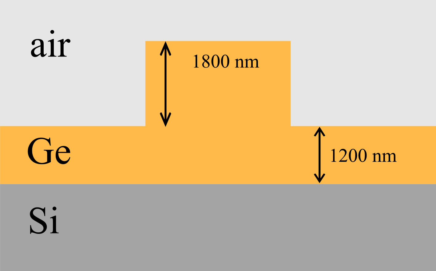
Layer stack of Cornerstone’s Ge-on-Si process.
Although technically a rib waveguide, it can be modeled as a wire waveguide because no surrounding trench is present. In this process, the Ge layer forms a continuous platform on top of Si, with the waveguide defined as a “wire” on that layer. For consistency with the Cornerstone repository, we retain the term “rib”.
To keep the PDK clean and maintainable, we remove unnecessary templates and adapt the generic_trace (renamed to trace.py in cornerstone_ge_on_si/ipkiss/cornerstone_ge_on_si/components/waveguides) to implement this single waveguide type.
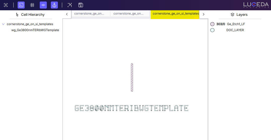
After adapting trace.py to the Cornerstone Ge-on-Si requirements, the resulting template is defined as follows:
class Ge3800nmTERibWGTemplate(WindowWaveguideTemplate):
    _name_prefix = "rib_Ge_3800nm_TE"
    _templated_class = TemplatedWindowWaveguide

    class Layout(WindowWaveguideTemplate.Layout):
        def _default_core_layer(self):
            return TECH.PPLAYER.Ge_Etch1_LF

        def _default_core_width(self):
            return TECH.WG.WIRE_WIDTH

        def _default_windows(self):
            core_hw = self.core_width / 2.0
            windows = [
                PathTraceWindow(
                    layer=self.core_layer,
                    start_offset=-core_hw,
                    end_offset=core_hw,
                ),
            ]
            return windows
For a detailed tutorial on trace templates, see Trace templates.
Finally, update traces.py in the technology folder by importing the Ge3800nmTERibWGTemplate. This step must be repeated for each trace template defined in the PDK.
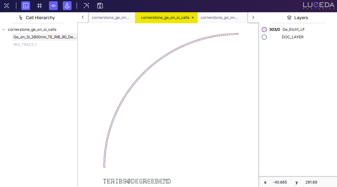
6. Add components
The PDK template generated from LCC includes a folder named dummy_pcell in the components directory. Components can be parametric (PCells) or fixed (without parameters).
To create an IPKISS PCell from a GDS file, we use i3.GDSCell.
This class allows referencing a specific cell within a GDS file and defining ports on the layout to enable circuit connectivity.
class TERib90DegreeBend(i3.GDSCell):
    """
    This component is a fixed GDS cell. You can use it as fixed_bend90 parameter in ConnectManhattan.
    This will insert this bend whenever a bend is required in routing.
    """

    _name_prefix = "Ge_on_Si_3800nm_TE_RIB_90_Degree_Bend"
    # this name will be the prefix in every instance of this class
    trace_template = i3.TraceTemplateProperty(doc="Trace template of the waveguide in this cell.")

    def _default_filename(self):
        path = os.path.dirname(__file__)
        # path to the gdsii file that contains the cell to be imported
        return os.path.join(path, "Ge_on_Si_3800nm_TE_RIB_90_Degree_Bend.gds")

    def _default_cell_name(self):
        return "Ge_on_Si_3800nm_TE_RIB_90_Degree_Bend"

    def _default_trace_template(self):
        return Ge3800nmTERibWGTemplate(name=self.name + "_tt")

    class Layout(i3.GDSCell.Layout):
        def generate(self, layout):
            layout = super().generate(layout)
            tt = self.trace_template

            layout += i3.OpticalPort(
                name="o1",
                position=(1.6, 0.0),
                trace_template=tt,
                angle=270,
            )

            layout += i3.OpticalPort(
                name="o2",
                position=(301.6, 300.0),
                trace_template=tt,
                angle=0.0,
            )
            return layout

    class Netlist(i3.NetlistFromLayout):
        pass
Note
If your PDK requires many components to be generated from GDS files, Luceda can assist in automating the creation of IPKISS PCells and port definitions from a GDS library. Please contact us for more information.
Note
Component PCells can also contain compact model to define the behaviour of the component in a circuit. This enables PDK users to run circuit simulations and verify their designs. These models can be analytical equations, based on physical simulation, or measurements. The Creating a First Circuit Simulation guide, provides a comprehensive instructions for model implementation.
All additional components should also be added to the components folder. While not strictly required, it is recommended to place each component in its own directory for clarity.
Complete the following checklist for each component, including the Cornerstone bend waveguide:
Create a directory named after the component and add empty __init__.py and pcell.py files.
Implement the component in pcell.py.
Update the [pdk_name]/iclib_export.yaml (here cornerstone_ge_on_si/iclib_export.yaml) to define how IPKISS Canvas symbols are generated for the new component.
Import the component in cornerstone_ge_on_si/ipkiss/cornerstone_ge_on_si/all.py and ensure it is listed in the __all__ variable.
For further details on component design, see Component Design Tutorial.
7. Adding transitions
In photonic circuit design, multiple waveguide types are often used within a single layout. When connecting these types, a transition (or taper) is required to join ports with different cross-sections. Abrupt changes in the waveguide profile can introduce loss or unwanted reflections. Transition PCells therefore provide an adiabatic transformation between cross-sections.
By defining transitions in the PDK and specifying the trace template pairs they apply to, IPKISS connectors can automatically insert the appropriate parametric transitions during routing.
The following implementation in cornerstone_ge_on_si/components/waveguides/transition.py defines a transition that is automatically inserted whenever waveguides with different trace templates are connected. This component dynamically computes the taper length based on the difference in core widths.
class LinearGeRibTransition(LinearWindowWaveguideTransition):
    """
    Transition between two ports with Ge3800nmTERibWGTemplate cross-sections. .
    """

    _name_prefix = "T_Rib_Rib_LIN"

    start_trace_template = RestrictedTraceTemplateProperty(Ge3800nmTERibWGTemplate)
    end_trace_template = RestrictedTraceTemplateProperty(Ge3800nmTERibWGTemplate)


class LinearGeRibTransitionFromPort(LinearGeRibTransition, LinearWindowWaveguideTransitionFromPort):
    class Layout(LinearGeRibTransition.Layout, LinearWindowWaveguideTransitionFromPort.Layout):
        def _default_length(self):
            # calculate taper length dynamically based on difference in core width
            w1 = self.start_trace_template.core_width
            w2 = self.end_trace_template.core_width
            a = 10.0
            return max(1.0, abs(a * (w2**2 - w1**2)))

        """Make sure we call the correct _generate_ports. The LinearWindowWaveguideTransitionFromPort
        knows how to position the end port based on the length of the transition."""
        _generate_ports = LinearWindowWaveguideTransitionFromPort.Layout._generate_ports
To enable this automation, the transition must be registered in the AutoTransitionDatabase within technology/transitions.py:
from ipkiss.technology import get_technology
from ..components.waveguides.transition import LinearGeRibTransitionFromPort


TECH = get_technology()
db = TECH.PCELLS.TRANSITION.AUTO_TRANSITION_DATABASE

db.default_if_identical = LinearGeRibTransitionFromPort
8. Documentation generation
This section explains how to manage and customize PDK documentation using the automated tools provided by IP Manager.
If the documentation exporter is enabled in the PDK configuration file (cornerstone_ge_on_si.cfg), documentation is generated automatically using the Sphinx engine, supporting both HTML and PDF formats. Custom content should be written in reStructuredText (.rst) format.
IP Manager provides extensions that keep documentation generation as automated as possible. Documentation for components, layers, and trace templates is extracted directly from the PDK.
layer table: extracts information from tech.yaml and inserts it into cornerstone_ge_on_si/docs/source/technology/index.rst.
- components: the component list at cornerstone_ge_on_si/docs/source/components/component_list.rst updates automatically.Additional details can be provided through docstrings in PCell class definitions.
class TERib90DegreeBend(i3.GDSCell):
    """
    This component is a fixed GDS cell. You can use it as fixed_bend90 parameter in ConnectManhattan.
    This will insert this bend whenever a bend is required in routing.
    """
Additional context and important information can be added to cornerstone_ge_on_si/docs/source/index.rst.
We strongly recommend tracking and documenting PDK updates in the in the changelog.rst file.
Customizing titles and component grouping:
Sphinx uses directives that mirror the component folder structure to organize items in the final documentation. By default, the folder name is used as the section title. This behavior can be overridden by adding a docstring to the __init__.py file within the folder.
This is particularly useful for grouping related components. For example, if a folder named dir_couplers contains multiple directional coupler cells, a docstring can be added to dir_couplers/__init__.py:
"""
Directional Couplers
====================

This section provides details and specifications for the
directional couplers included in the Cornerstone Ge-on-Si PDK.
"""
With this docstring, Sphinx groups all files within the directory under the heading “Directional Couplers” and includes the introductory text.
9. Inspection and building
At this stage, the PDK can be inspected and built iteratively until it meets the desired requirements.
build.py
Generates a distributable library from the PDK source. The resulting build is stored in the cornerstone_ge_on_si/builds directory.
inspect.py
Allows verification of both zipped and unzipped builds. It visualizes three core elements in the layout viewer:
Layers
Components
Trace templates
Once inspection is complete and the PDK is finalized, the build can be distributed to users. Designers can integrate the PDK into their environment by installing it via the Luceda Control Center.
10. Quality assurance
To maintain PDK quality, regression tests should be executed regularly. This helps detect unintended changes or regressions in functionality.
For a detailed guide, see Regression testing.