OpenWireWgAperture
- class awg_designer.all.OpenWireWgAperture
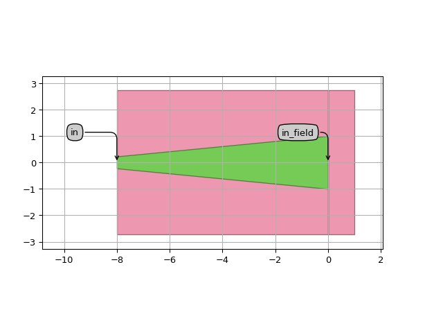
An aperture tapering from a wire waveguide to the Slab opening.
Uses the standard picazzo WireWaveguideTemplate.
- Parameters:
- slab_template: PCell and SlabTemplate, required
template for free propagation region
- transition: PCell
- field_ports:
list of regular ports that have field ports
- trace_template: PCell and _TraceTemplate
template of the start waveguide
- name: String that contains only ISO/IEC 8859-1 (extended ASCII py3) or pure ASCII (py2) characters
The unique name of the pcell
- Other Parameters:
- aperture_trace_template: PCell and _TraceTemplate, locked
template of the aperture cross-section
Views
- class Layout
- Parameters:
- aperture_edge_width: float and number > 0
width of the cladding edges at the opening of the aperture
- aperture_core_width: float and number > 0
width of the waveguide core at the opening of the aperture
- transition_parameters:
dict of parameters for the aperture transition
- fpr_depth: float and number > 0
depth of the virtual free propagation region
- width: float and number > 0
width of the aperture
- transition_length: float and number > 0
transition length
- center: Coord2
center coordinate
- front_shape: Shape
Shape of the ‘front’ of the aperture, where the light comes out
- view_name: String that contains only alphanumeric characters from the ASCII set or contains _$. ASCII set is extended on PY3.
The name of the view
- Other Parameters:
- slab_layers: locked
list of layers that should be drawn as exclusion zone
Examples
import si_fab.all as pdk  # noqa: F401
from awg_designer import all as filters
import ipkiss3.all as i3
import numpy as np

slab_soi = filters.SlabTemplate(name="SOI_Template")
slab_soi.Layout(slab_layers=[i3.PPLayer(i3.TECH.PROCESS.WG, i3.TECH.PURPOSE.DF_AREA)])
slab_soi.SlabModes(
    modes=[
        filters.InterpolatedSlabMode(
            name="TE0",
            wavelengths=np.linspace(1.2, 1.6, 5),
            n_effs=np.array([3.0568, 2.9866, 2.9223, 2.8617, 2.8042]),
            polarization="TE",
        )
    ]
)
w_ap = 2.0
ap_wire = filters.OpenWireWgAperture(slab_template=slab_soi)
ap_wire_lo = ap_wire.Layout(aperture_core_width=w_ap, transition_length=8.0)
ap_wire_lo.visualize(annotate=True)

- class FieldModelFromFunction
This FieldModel retrieves the field from a given function. The aperture transmission is 1, and reflection is 0. This can be overridden by defining your own CircuitModelView on the aperture.
For more information about field models see the Apertures doc.
- Parameters:
- field_width: float and number > 0
Extent of the field to consider (two-sided).
- field_function:
Callable f(x, center) that returns an array of field values,given the 1 dimensional coordinates x along the aperture facet, centered around center.
- positions: Shape
coordinates, in the local reference frame of the aperture, of the fields
- netlist_view: NetlistView
- layout_view: _LayoutView
- n_o_passes: int and number > 0
number of simulation passes
- space: _SlabPropagationEngine.Space
Space with all the elements representing the PCell
- engine: _SlabPropagationEngine
Slab simulation engine
- slab_modes: SlabModeDict
dict of Slab Modes
- view_name: String that contains only alphanumeric characters from the ASCII set or contains _$. ASCII set is extended on PY3.
The name of the view
See also
gaussian_fieldFunction to define a gaussian field.
OpenTransitionAperture.FieldModelFromCamfrWill automatically run camfr simulations to calculate the mode profile.
Examples
import si_fab.all as pdk  # noqa: F401
from awg_designer import all as filters
from functools import partial
from pysics.basics.environment import Environment
import ipkiss3.all as i3
import numpy as np

slab_soi = filters.SlabTemplate(name="SOI_Template")
slab_soi.Layout(slab_layers=[i3.PPLayer(i3.TECH.PROCESS.WG, i3.TECH.PURPOSE.DF_AREA)])
slab_soi.SlabModes(
    modes=[
        filters.InterpolatedSlabMode(
            name="TE0",
            wavelengths=np.linspace(1.2, 1.6, 5),
            n_effs=np.array([3.0568, 2.9866, 2.9223, 2.8617, 2.8042]),
            polarization="TE",
        )
    ]
)
w_ap = 2.0
ap_wire = filters.OpenWireWgAperture(slab_template=slab_soi)
ap_wire.Layout(aperture_core_width=w_ap, transition_length=8.0)

gaussian = partial(filters.gaussian_field, waist=1.1)
ap_wire_sm = ap_wire.FieldModelFromFunction(field_function=gaussian)
environment = Environment(wavelength=1.55)
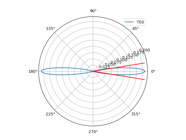
ff = ap_wire_sm.get_far_field(environment=environment)
ff.visualize()
# alpha: spreading angle of the aperture, typically taken
# somewhere 1.4 - 1.7 x the divergence angle of the mode.
alpha = 1.4 * ff.divergence_angle()  # noqa:F841

- class FieldModelFromCamfr
Field model calculating the output fields as a CAMFR simulation progating from the input port to the field port. The aperture transmission and reflection values are calculated from a CAMFR eigenmode propagation simulation.
For more information about field models see the Apertures doc.
- Parameters:
- material_stack_to_material_map: ( dict ), *None allowed*
Effective materials for each stack used in the virtual fabrication.
- process_flow: VFabricationProcessFlow
Virtual fabrication process flow to use.
- core_z_window: tuple2 and Tuple of <class ‘float’>
Window which describes the z-range of the core layer.
- simulation_window: SizeInfo
SizeInfo which describes the region of the layout to simulate.
- positions: Shape
coordinates, in the local reference frame of the aperture, of the fields
- netlist_view: NetlistView
- layout_view: _LayoutView
- n_o_passes: int and number > 0
number of simulation passes
- space: _SlabPropagationEngine.Space
Space with all the elements representing the PCell
- engine: _SlabPropagationEngine
Slab simulation engine
- slab_modes: SlabModeDict
dict of Slab Modes
- view_name: String that contains only alphanumeric characters from the ASCII set or contains _$. ASCII set is extended on PY3.
The name of the view
Examples
import si_fab.all as pdk  # noqa: F401
from awg_designer import all as filters
from pysics.basics.environment import Environment
import ipkiss3.all as i3
import numpy as np

slab_soi = filters.SlabTemplate(name="SOI_Template")
slab_soi.Layout(slab_layers=[i3.PPLayer(i3.TECH.PROCESS.WG, i3.TECH.PURPOSE.DF_AREA)])
slab_soi.SlabModes(
    modes=[
        filters.InterpolatedSlabMode(
            name="TE0",
            wavelengths=np.linspace(1.2, 1.6, 5),
            n_effs=np.array([3.0568, 2.9866, 2.9223, 2.8617, 2.8042]),
            polarization="TE",
        )
    ]
)
w_ap = 2.0
ap_wire = filters.OpenWireWgAperture(slab_template=slab_soi)
ap_wire.Layout(aperture_core_width=w_ap, transition_length=8.0)
ap_wire_sm = ap_wire.FieldModelFromCamfr()
environment = Environment(wavelength=1.55)
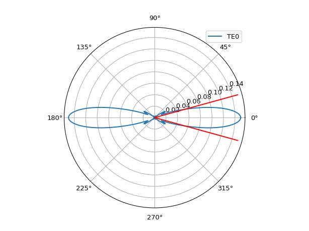
ff = ap_wire_sm.get_far_field(environment=environment)
ff.visualize()
# alpha: spreading angle of the aperture, typically taken
# somewhere 1.4 - 1.7 x the divergence angle of the mode.
alpha = 1.4 * ff.divergence_angle()  # noqa: F841

- class CircuitModel
- Parameters:
- slabfield_view: _SlabFieldModelView
- simulation_wavelengths: ( list<int, float, integer, floating and number > 0> ), *None allowed*
Wavelengths for which to simulate the underlying physical model.Defaults to None, in which case a physical simulation will be done for each requested wavelength.If a single wavelength is specified, the model will be wavelength independent.If multiple wavelengths are given, only these wavelengths are valid.
- reflection: int, float, number, complex
Complex reflection of the aperture
- layout_view: ( _LayoutView ), *None allowed*
- netlist_view: ( NetlistView ), *None allowed*
- view_name: String that contains only alphanumeric characters from the ASCII set or contains _$. ASCII set is extended on PY3.
The name of the view
- Other Parameters:
- solver: str and String that contains only ISO/IEC 8859-1 (extended ASCII py3) or pure ASCII (py2) characters, locked
circuit solver to use