Introduction
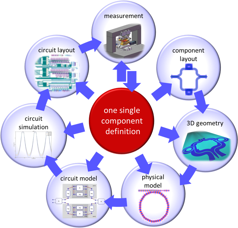
Photonic design happens at many different levels. A lot of the component design is still done using detailed electromagnetic simulations, tailoring geometries to a very detailed level. At the same time, circuit design requires abstraction at a much higher level. Traditionally, these different steps in the design flow require very different tools, while at the heart they require the same component definition: at the end of your design you want the correct components to be placed on the mask for fabrication. IPKISS integrates the different aspects of photonic design into one framework, where you can define your component once as a parametric cell (PCell) and then use it throughout your design process:
performing electromagnetic simulations,
defining circuit models,
connecting devices into a circuit,
running circuit simulations,
verify functionality (post-layout circuit simulation) and connectivity (IPKISS Canvas),
automate the testing of your devices at all stages of the design cycle,
generate the mask layout that will be sent to the fab,
and finally even process the testing of the fabricated devices.
Because the same component definition is used in the entire flow, design errors are significantly reduced. Also, the level of automation that can be achieved with this flow can enable more efficient and error-proof design flows.

IPKISS enables you to use the same component definition throughout the design flow.
IPKISS comes with several design kits already included, so you can start designing today! There are a range of open source Process Design Kits (PDKs) as well as SiFab, a stand-alone Luceda PDK that imitates a real silicon foundry. It contains a complete technology tree, as well as many common components such as waveguides, modulators, crossings and grating couplers. You can use to start learning how to design in IPKISS, or as a starting point to develop your own components or PDK.
Python Scripting
At the core of IPKISS is a powerful Python scripting framework. We opted for a scripting layer because it poses the minimum of constraints. The Python language is easy to read, is an accepted industry-standard, and comes with a rich ecosystem of scientific and engineering packages. Moreover, it makes IPKISS an open environment, where it is possible to integrate different design and simulation tools (even from other tool vendors) into your design flow. Python scripting is at the core of many PIC design activities: building parametric cells (PCells) and design IP, launching device simulations, generating full PIC layouts, running circuit simulations, verifying the correctness of your designs and so on.
Graphical assistance using IPKISS Canvas
In parallel with the Python code, users can also use IPKISS Canvas, a Graphical User Interface (GUI) that acts as a copilot to your PIC design activities. IPKISS Canvas assists you in capturing schematics, generating Python code, verifying designs and so on. The code generation reduces the barrier to entry for those not yet familiar with the platform, and acts as a starting point for further Python coding. IPKISS also has powerful connection extraction routines (both optical + electrical) that allow to verify the connectivity and correctness of your layouts in Canvas, prior to tape-out.
History
IPKISS development originated at Ghent University and imec in 2002, to enable mask design of large silicon photonics circuits, which was difficult with any of the tools at that time. Over time, the framework evolved into much more than layout, incorporating multiple simulations tools (electromagnetic and circuit) and an entire test & measurement framework. In 2012, a limited version of IPKISS was open sourced, and was widely used for many tape-outs of silicon photonic chips. In 2014, Luceda Photonics was incorporated to bring the development of IPKISS up to industry standards and provide commercial support and services. This resulted in a major upgrade of the software that fully integrates layout and simulation and enables the integration with electronic design flows.
By now, IPKISS is the design tool of choice of a large base of designers world-wide and has been validated on many photonic IC foundry technologies including various silicon photonics, silicon nitride and indium phosphide based platforms. Assembly design kits are made available to assist the user in making chips that are easily packaged and tested.
Note
The name IPKISS is not chosen as an acronym, although you could come up with meaningful expansions such as Integrated Photonics: Keep It Simple Stupid (although we’re not that fond of the last word at Luceda Photonics). The origin of the name lies in the original purpose of the framework, which was making really complex photonic mask layouts. IPKISS was named after Stanley Ipkiss, the key character in the comic books The Mask (and the movie with Jim Carrey). The name just stuck; we like it. The name of the PICAZZO component library is a tongue-in-cheek to the artist Pablo Picasso, who, during a period in his life, was an enthusiastic painter of masks.